利用时域TDR分析RFIC与PCB绑定金丝互连仿真

射频百花潭 2021-09-30 09:08

在本应用说明中,我们将使用Empire XPU模拟和脉冲激励的时域结果来理解和优化从芯片到PCB的绑定过渡。该方法提供了沿信号路径的不连续位置的详细信息。使用过时域反射仪(TDR)分析方法:当脉冲沿着信号路径传播时,使用脉冲激励来研究反射和传输电压与时间的关系要,在任何阻抗不连续处,反射信号的幅度告诉我们线路阻抗的变化。传输路径分辨率取决于脉冲的带宽。基于IHP SG13S堆叠,使用一个简单的RFIC模型进行演示。本应用说明的主要目的是展示分析工作流程–设计示例。

The test circuit


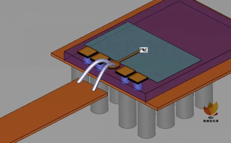
Baseline model for this appnote is a 300µm thick chip placed inside a recessed cutout of the 254µm PCB, to minimize interconnect length. Wire bonds are used to connect the RF line as well as the multiple grounds. Pad size for the ground pads is 80µm with 20µm spacing.

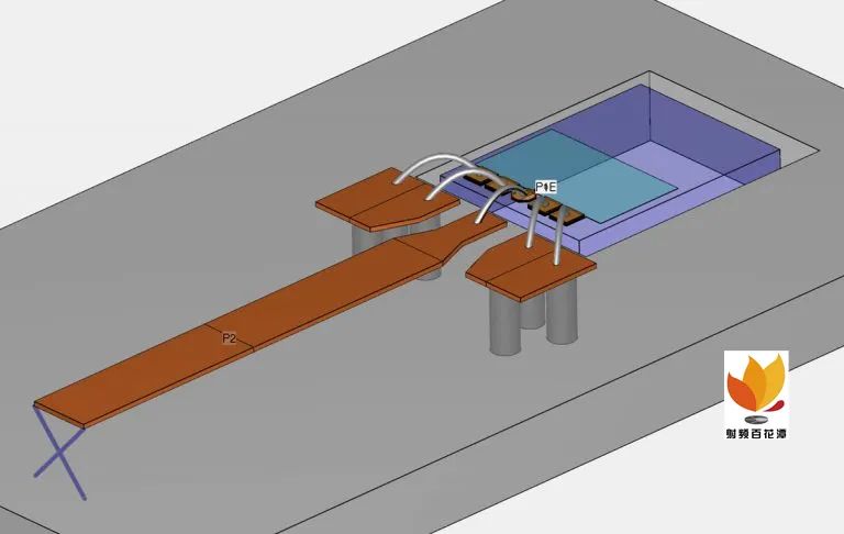
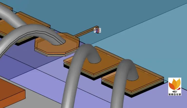
On chip, a lumped vertical port from TopMetal2 to Metal1 is used. The blue RF ground polygon on Metal 1 is approx. 10µm below the pads, so we have a nice short connection to all signal and ground pads. (Note to the GaAs designers: this SiGe stackup is different from GaAs, we don’t have the chip backside as the RF ground.)

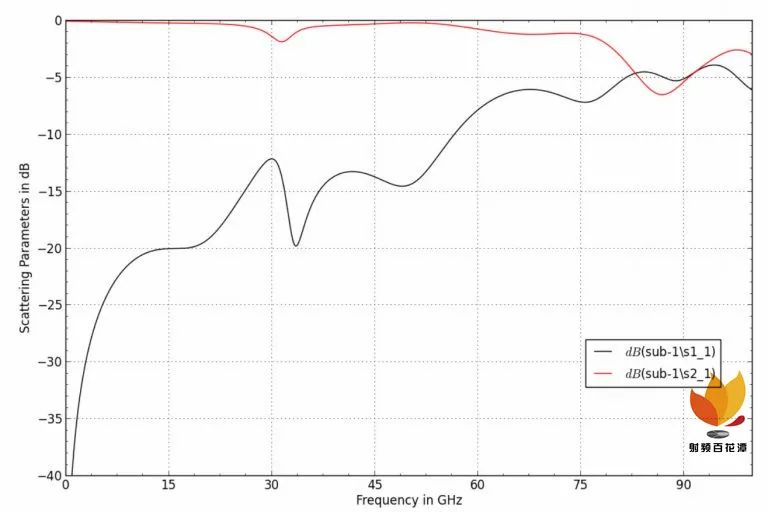
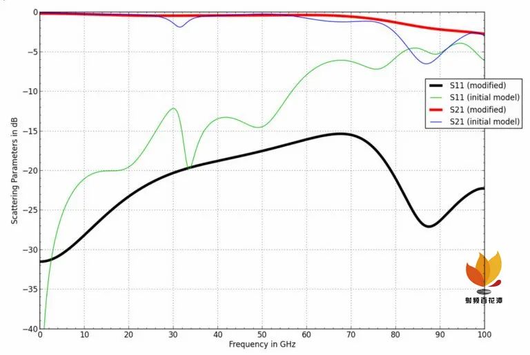
This results in rather poor RF performance as shown below:

Now the question is: what are the reasons for this poor matching, is it just the bond wire inductance? How to improve the response? This is where time domain results for pulse excitation are useful, to localized the discontinuities.


Test circuit time analyzed with time domain pulse


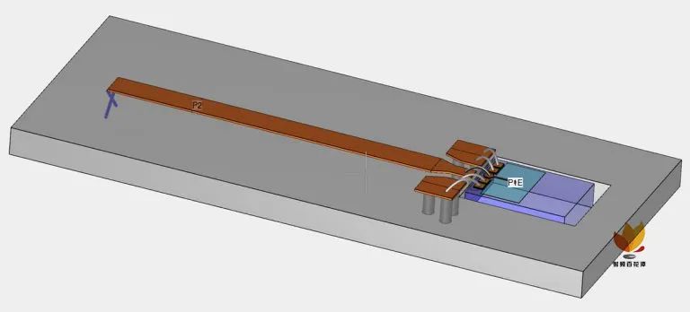
To help with an initial understanding of the time domain results, we have stretched the microstrip line on PCB. This results in a longer time delay until the signal from the chip reaches port 2 on the PCB, and we can study the reflections from the interconnect more easily.

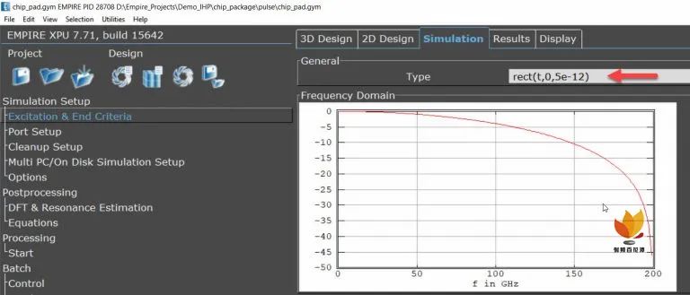
For excitation at port 1 on chip, we use a square pulse with 5ps duration, instead of the default gaussian pulse that is used for S-parameter simulations.

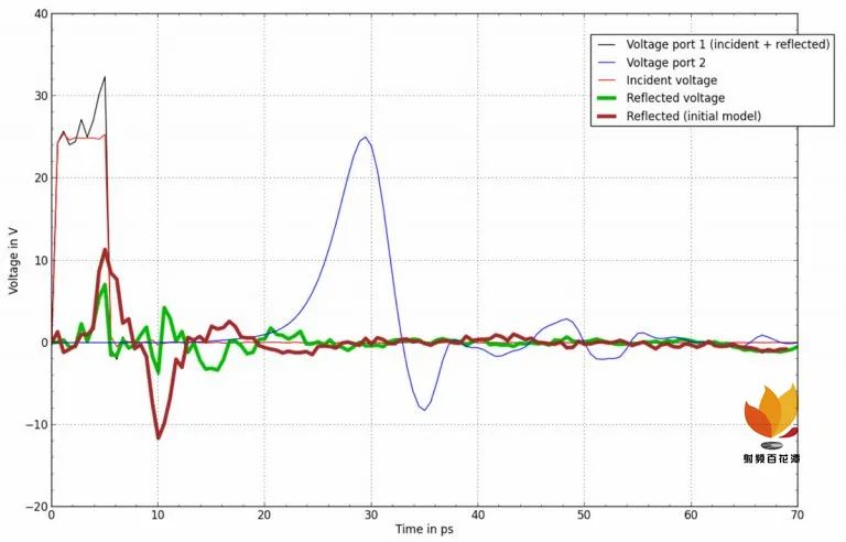
Simulation results for the time domain signal are shown below, plotted over time. Red is the incident voltage that we have defined in the excitation, green is the reflected voltage, black is the total instantaneous voltage at port 1 (incident + reflected) and blue is the voltage at port 2. We can see the time delay of the transmission of around 28ps, with a low pass response that takes out the fast slope from our initial square signal.

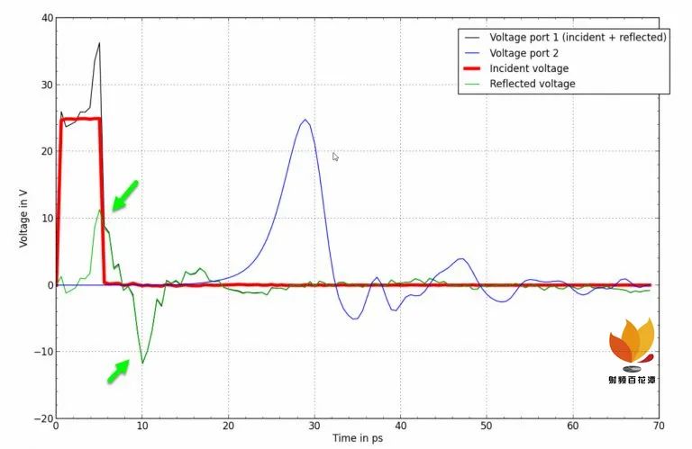
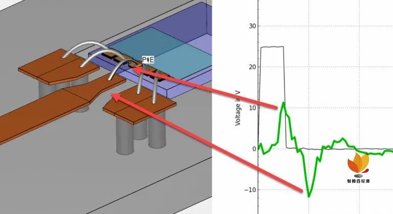
The green curve shows a positive reflection (line impedance increase) at 5ps delay and a negative reflection (line impedance decrease) at 10ps delay. This is the main issue that we need to solve. Looking at the geometry and related electrical length, we can identify that the positive peak is the bond wire (too much series inductance) and the negative peak is the pad at the end of the bond wire on PCB (too much shunt capacitance between signal and ground).


Improving the layout


Now that we have identified these two issues, we can think about counter measures: by changing the ground connection from wire bond to TSV, we can get rid of the ground pads that are near the signal pad on PCB. This reduces the shunt capacitance between signal and ground. It also enables us to increase signal line width at the bond (with having extra capacitance from small gap) and then have two bond wires for the signal path, instead of one.

TSV require a reduced chip thickness of 75µm, so the chip is now placed onto the PCB top side, without recessed mounting.

In time domain, we can see a strong reduction of the reflected signal (green) compared to the previous model (brown): The positive peak from bond wire inductance is much reduced, and the negative peak from the excess capacitance at the PCB landing pad is almost gone. So we expect a much better wideband performance now.


When evaluating the model for S-parameters, this is indeed confirmed, with much better return loss at higher frequencies:


Why use time domain EM simulation?


Here, we use a time domain EM solver (Empire XPU) with direct pulse excitation in the time domain. This enables EM simulation with very short pulses, resulting in very high spatial resolution of discontinuities.

An alternative method would be EM simulation in the frequency domain (FEM or MoM) where S-parameters are simulated first, and time domain analysis is done by fourier transform of the S-parameters. In that case, we would need very wideband S-parameters to realize such short pulses (5ps pulse with <1ps rise time) for high spatial resolution.

Summary


In this appnote, we have seen how TDR-like simulation methods, with evaluation of pulses in the time domain, can help to improve wide band response of interconnects. This type of simulation is easily done in Empire XPU by switching from the default gaussian excitation (useful for S-parameter simulation) to user defined excitation. Simulation times are very short using this method, because the FDTD method uses direct simulation in the time domain. Simulation time was less than 3 minutes on a Core i9 desktop PC, using 3 million mesh cells.

If needed, a more complex time signal could also be used for simulation, or an excitation signal with controlled rise time. However, for this “computed TDR” analysis the fast square wave signal seemed most useful.

声明:


本号对所有原创、转载文章的陈述与观点均保持中立,推送文章仅供读者学习和交流。文章、图片等版权归原作者享有。

投稿/招聘/推广/宣传 请加微信:15989459034

射频百花潭 国内最大的射频微波公众号,专注于射频微波/高频技术分享和信息传递!
评论 (0)
  •   无人机电磁兼容模拟训练系统软件:全方位剖析   一、系统概述   北京华盛恒辉无人机电磁兼容模拟训练系统软件,专为满足无人机于复杂电磁环境下的运行需求而打造,是一款专业训练工具。其核心功能是模拟无人机在电磁干扰(EMI)与电磁敏感度(EMS)环境里的运行状况,助力用户评估无人机电磁兼容性能,增强其在复杂电磁场景中的适应水平。   应用案例   目前,已有多个无人机电磁兼容模拟训练系统在实际应用中取得了显著成效。例如,北京华盛恒辉和北京五木恒润无人机电磁兼容模拟训练系统。这些成功案例为
    华盛恒辉l58ll334744 2025-04-17 14:52 33浏览
  •   无人机蜂群电磁作战仿真系统全解析   一、系统概述   无人机蜂群电磁作战仿真系统是专业的仿真平台,用于模拟无人机蜂群在复杂电磁环境中的作战行为与性能。它构建虚拟电磁环境,模拟无人机蜂群执行任务时可能遇到的电磁干扰与攻击,评估作战效能和抗干扰能力,为其设计、优化及实战应用提供科学依据。   应用案例   目前,已有多个无人机蜂群电磁作战仿真系统在实际应用中取得了显著成效。例如,北京华盛恒辉和北京五木恒润无人机蜂群电磁作战仿真系统。这些成功案例为无人机蜂群电磁作战仿真系统的推广和应用提
    华盛恒辉l58ll334744 2025-04-17 16:29 69浏览
  • 现阶段,Zigbee、Z-Wave、Thread、Wi-Fi与蓝牙等多种通信协议在智能家居行业中已得到广泛应用,但协议间互不兼容的通信问题仍在凸显。由于各协议自成体系、彼此割据,智能家居市场被迫催生出大量桥接器、集线器及兼容性软件以在不同生态的设备间构建通信桥梁,而这种现象不仅增加了智能家居厂商的研发成本与时间投入,还严重削减了终端用户的使用体验。为应对智能家居的生态割裂现象,家居厂商需为不同通信协议重复开发适配方案,而消费者则需面对设备入网流程繁琐、跨品牌功能阉割及兼容隐患等现实困境。在此背景
    华普微HOPERF 2025-04-17 17:53 49浏览
  • 近日,全球6G技术与产业生态大会(简称“全球6G技术大会”)在南京召开。紫光展锐应邀出席“空天地一体化与数字低空”平行论坛,并从6G通信、感知、定位等多方面分享了紫光展锐在6G前沿科技领域的创新理念及在空天地一体化技术方面的研发探索情况。全球6G技术大会是6G领域覆盖广泛、内容全面的国际会议。今年大会以“共筑创新 同享未来”为主题,聚焦6G愿景与关键技术、安全可信、绿色可持续发展等前沿主题,汇聚国内外24家企业、百余名国际知名高校与科研代表共同商讨如何推动全行业6G标准共识形成。6G迈入关键期,
    紫光展锐 2025-04-17 18:55 127浏览
  •   北京华盛恒辉无人机电磁兼容模拟训练系统软件是专门用于模拟与分析无人机在复杂电磁环境中电磁兼容性(EMC)表现的软件工具。借助仿真技术,它能帮助用户评估无人机在电磁干扰下的性能,优化电磁兼容设计,保障无人机在复杂电磁环境中稳定运行。   应用案例   目前,已有多个无人机电磁兼容模拟训练系统在实际应用中取得了显著成效。例如,北京华盛恒辉和北京五木恒润无人机电磁兼容模拟训练系统。这些成功案例为无人机电磁兼容模拟训练系统的推广和应用提供了有力支持。   系统功能   电磁环境建模:支持三维
    华盛恒辉l58ll334744 2025-04-17 15:10 52浏览
  •   无人机蜂群电磁作战仿真系统软件,是专门用于模拟、验证无人机蜂群在电磁作战环境中协同、干扰、通信以及对抗等能力的工具。下面从功能需求、技术架构、典型功能模块、发展趋势及应用场景等方面展开介绍:   应用案例   目前,已有多个无人机蜂群电磁作战仿真系统在实际应用中取得了显著成效。例如,北京华盛恒辉和北京五木恒润无人机蜂群电磁作战仿真系统。这些成功案例为无人机蜂群电磁作战仿真系统的推广和应用提供了有力支持。   功能需求   电磁环境建模:模拟构建复杂多样的电磁环境,涵盖各类电磁干扰源与
    华盛恒辉l58ll334744 2025-04-17 16:49 62浏览
  • 置信区间反映的是“样本均值”这个统计量的不确定性,因此使用的是标准误(standard error),而不是直接用样本标准差(standard deviation)。标准误体现的是均值的波动程度,而样本标准差体现的是个体数据的波动程度,两者并非一回事,就如下图所显示的一样。下面优思学院会一步一步解释清楚:一、标准差和标准误,究竟差在哪?很多同学对“标准差”和“标准误”这两个概念傻傻分不清楚,但其实差别明显:标准差(Standard Deviation,σ或s):是衡量单个数据点相对于平均值波动的
    优思学院 2025-04-17 13:59 24浏览
  • 1. 在Ubuntu官网下载Ubuntu server  20.04版本https://releases.ubuntu.com/20.04.6/2. 在vmware下安装Ubuntu3. 改Ubuntu静态IP$ sudo vi /etc/netplan/00-installer-config.yaml# This is the network config written by 'subiquity'network:  renderer: networkd&nbs
    二月半 2025-04-17 16:27 66浏览
  •   无人机电磁环境效应仿真系统:深度剖析   一、系统概述   无人机电磁环境效应仿真系统,专为无人机在复杂电磁环境下的性能评估及抗干扰能力训练打造。借助高精度仿真技术,它模拟无人机在各类电磁干扰场景中的运行状态,为研发、测试与训练工作提供有力支撑。   应用案例   目前,已有多个无人机电磁环境效应仿真系统在实际应用中取得了显著成效。例如,北京华盛恒辉和北京五木恒润无人机电磁环境效应仿真系统。这些成功案例为无人机电磁环境效应仿真系统的推广和应用提供了有力支持。   二、系统功能  
    华盛恒辉l58ll334744 2025-04-17 15:51 64浏览
  • 一、行业背景与需求智能门锁作为智能家居的核心入口,正从单一安防工具向多场景交互终端演进。随着消费者对便捷性、安全性需求的提升,行业竞争已从基础功能转向成本优化与智能化整合。传统门锁后板方案依赖多颗独立芯片(如MCU、电机驱动、通信模块、语音模块等),导致硬件复杂、功耗高、开发周期长,且成本压力显著。如何通过高集成度方案降低成本、提升功能扩展性,成为厂商破局关键。WTVXXX-32N语音芯片通过“单芯片多任务”设计,将语音播报、电机驱动、通信协议解析、传感器检测等功能整合于一体,为智能门锁后板提供
    广州唯创电子 2025-04-18 09:04 111浏览
  • 一、行业背景与需求随着智能化技术的快速发展和用户对便捷性需求的提升,电动车行业正经历从传统机械控制向智能交互的转型。传统电动车依赖物理钥匙、遥控器和独立防盗装置,存在操作繁琐、功能单一、交互性差等问题。用户期待通过手机等智能终端实现远程控制、实时数据监控及个性化交互体验。为此,将蓝牙语音芯片集成至电动车中控系统,成为推动智能化升级的关键技术路径。二、方案概述本方案通过在电动车中控系统中集成WT2605C蓝牙语音芯片,构建一套低成本、高兼容性的智能交互平台,实现以下核心功能:手机互联控制:支持蓝牙
    广州唯创电子 2025-04-18 08:33 97浏览
  • 【摘要/前言】4月春日花正好,Electronica就在浪漫春日里,盛大启幕。2025年4月15-17日,慕尼黑上海电子展于上海新国际博览中心成功举办。伴随着AI、新能源汽车、半导体的热潮,今年的Electronica盛况空前。请跟随Samtec的视角,感受精彩时刻!【 Samtec展台:老虎的朋友圈技术派对】借天时、占地利、聚人和,Samtec 展台人气爆棚!每年展会与大家相聚,总能收获温暖与动力~Samtec展台位于W3展馆716展位,新老朋友相聚于此,俨然一场线下技术派对!前沿D
    电子资讯报 2025-04-17 11:38 34浏览
我要评论
0
0
点击右上角,分享到朋友圈 我知道啦
请使用浏览器分享功能 我知道啦