关于clock gating 已经写过:《clock gating | 从ICG cell 在 library 中的定义说起》《clock gating | Gating 的插入与验证》《clock gating | clock gating 的timing check》《clock gating | ODC-based Clock Gating》。最近在学习Joules 20.1 update training 时又接触到了两个新概念:combinational clock gating 跟 sequential clock gating, 觍着老脸去问研发大爷这是啥,大爷说:你丫不能自己谷歌一下吗?于是在ElectronicDesign 上找到了一篇好文章,深入简出地描述了两者的区别。
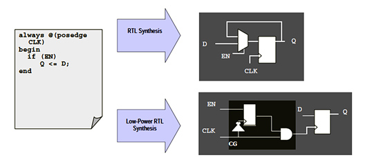
概括来说,combinational clock gating 就是通常所说的clock gating, 它不改变电路的逻辑功能,对设计实现影响没有,但是它只能省掉clock 的多余toggle. 
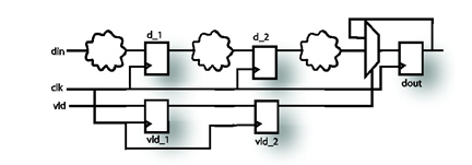
Sequential clock gating 的搜索空间更大,在时序路径多级寄存器之间进行分析,找到所有冗余的翻转,该类Gating 通常有两种:- observability-based clock gating, writes done to a register are unobservable down-stream. Following is an example of the first type, where under some conditions, writes to a register will never be observed at the design output. If the signal vld_2 is low in a particular cycle, the register dout retains its older value. This means that writes that would have happened in register d_2, one cycle back and in d_1, two cycles back are redundant. Observability-based clock gating identifies this redundant write and adds a suitable gating condition based on the vld signal.

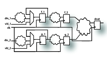
- stability-based clock gating, writes requires multi-cycle analysis of the design. Following shows an example of the second type of redundant writes. This is where the same value gets written to registers across consecutive clock cycles. When the signals vld_1 and vld_2 are low, registers f_1 and g_1 retain their previously held values. Consequently, values written into registers f_2 and g_2 in the next clock cycle are identical to what was written into them in the previous cycle. Stability-based clock gating identifies the redundant write and adds a suitable gating condition using a one-cycle delayed version of vld_1 for f_2 (and similarly, a one-cycle delayed version of vld_2 for g_2).

下面一部分原文照办,包括:
如何分析设计找到可以插入Sequential clock gating 的点。
Sequential clock gating 可以多省哪些power.
Sequential clock gating 对设计验证有哪些影响。
目前业界如何做Sequential clock gating.
Identifying Sequential Clock Gating Opportunities
Combinational clock gating has been part of RTL synthesis tools for several years and has become dependable for optimizing for power. Very rarely do synthesis tools miss a combinational clock gating opportunity. Yet, in certain cases the self-assignment to a register uses complex logic (either spanning multiple design hierarchies or written as separate functions) that may cause difficulties for RTL synthesis tools in identifying combinational clock gating. In such cases, designers simplify the complex logic and rewrite it as an “if” statement on the register assignment, thereby simplifying the job of RTL synthesis tools. However, identifying sequential clock gating opportunities is beyond the scope of RTL synthesis tools. Power conscious designers try to analyze the registers for redundant accesses (unobservable or stable writes) and look for conditions under which such accesses can be shut off. There is no single known method of achieving this, and designers mostly develop this expertise over time. Even so, the process can get very tedious and error prone without suitable assistance.Sequential clock-gating tools introduced to the market either aid the manual exploration of sequential clock gating opportunities or do it automatically. Designers pick the desired methodology (manual versus automated) based on their schedule and comfort with letting a tool make the decisions for them. The tool must fulfill some requirements to make the job of an RTL designer easier, regardless of whether it is used in an automated or manual exploration mode:- Early feedback about possible total power savings through the elimination of redundant writes to registers
- Clock gating expressions and directions about how to put them into the RTL and additionally, provide a way to change the expressions so that users can configure them to suit their requirements (ease of patching, size of expression, etc.)
- Accurate estimates of power savings and area cost for the clock gating expressions
- If the tool misses creating some clock gating expressions, then feedback must be provided to the user about the potential power savings and the changes (RTL, tool constraints, etc.) that the user can make to help realize those expressions
Such a flow will inform the designer very early on whether a significant potential for power optimization exists in the design. If not, the designer can focus solely on objectives like area and performance. The level of scope will also indicate how much effort should be put towards power optimization. Since the designer understands the power impact of each potential change (putting in a clock gating expression, an RTL or constraints change, the registers with most power saving potential, etc.), the designer can prioritize changes based on delivery schedule. On completion of the sequential clock gating tool’s run, the designer will know how much of the total potential power savings has been realized for the design.
Impact of Sequential Clock Gating on Power
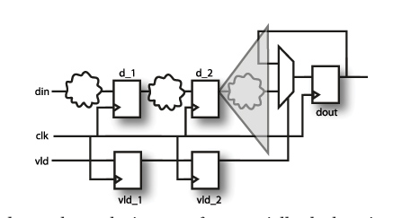
Estimating the power saving potential of a combinational clock gating expression is relatively easy. The change in power of a clock-gated register is computed after reducing the switching activity of the clock net driving the register. The signal that disables the clock net is present in the design, and it is easy to compute its impact on the switching of the clock net by using combinational switching activity propagation techniques. However, sequential clock gating alters the sequential nature of the design. For example, to perform observability-based clock gating for the circuit shown in Figure 2, signal vld_1 will be used to gate the clock going to register d_2. This will not only change the clock toggles but also the toggle activity at the output of register d_2, which in turn will impact switching activity of the entire fanout of register d_2. Following shows the region (shaded) where switching activity would change as a result of sequentially clock gating register d_2. If only the impact on register power is reported, then a potentially good clock gating expression (since it could have saved a large amount of datapath power) might get rejected.

Hence, to compute accurate power, switching activities for all affected signals and new signals need to be computed. The tool must take the actual power saving impact of a sequential clock gating change into account while making optimization decisions or when presenting the opportunity to the user. An automated tool has to evaluate hundreds and thousands of such gating expressions, so the power computation must be very quick, and at the same time the accuracy of computation should not be compromised.
Verification Impact
The act of combinational clock gating does not change the functionality of the registers in the design, and hence, traditional logical equivalence checkers (LEC) can be used to verify the correctness of such clock gating transformations. Sequential clock gating, on the other hand, changes the sequential nature of the design. For example, if register d_2 in Figure 2 is gated using signal vld_1, then its output is no longer identical to the original design. However, the design output remains unchanged. Traditional LEC tools cannot verify the equivalence of such changes since they require that the register behavior of the two designs being verified is identical. Sequential logic equivalence checkers (SLEC) on the market can help verify the correctness of sequential changes made to the design (like pipelining, retiming, rescheduling, clock gating, etc.). Such tools can be deployed to verify the correctness of sequential clock gating changes. Users must be aware of the following requirements for verifying the correctness of clock gating changes:
The optimization tool itself cannot make claims about the correctness of the changes it makes
The verification tool should be able to independently verify the correctness of sequential changes made to the design (either by automation or manually)
Verification should be fast and formal
Simulation vector-based verification cannot guarantee the correctness of sequential changes since the bug could be several cycles deep and could remain undetected
Design Flow Support
Combinational clock gating is already present as an internal optimization step in all RTL synthesis tools. RTL synthesis tools themselves support various design flow requirements: bottom-up, engineering change orders (ECO), etc. However, sequential clock gating is still an intermediate stage in the design flow. Either the designer is doing it manually or an automated tool is making such changes to the RTL. For an automated tool, the requirements for writing changed RTL include: complete support for all HDLs (SystemVerilog, Verilog, VHDL, etc.) and a mix thereof;minimal changes to the RTL (preserve all user comments, formatting, and pre-processor directives like macros, defines, includes, etc.); comprehensive configurability of the written-out RTL so as to support Lint rule requirements specific to individual design houses; and clock gating changes written in such a way that they are understood and honored by RTL synthesis tools.
If the sequential clock gating tool is sitting in an automated design flow, then it needs to provide the complete support for ECOs. An ECO change in the RTL could potentially make some of the optimizations done by the automated tool invalid. The requirements for an automated tool for ECO support are:
Only drop those optimizations which are invalid, and no more
The output RTL should be identical to the RTL output from the previous run (other than the changes required to make some optimizations invalid)
Clear directives on how the invalidation of some optimizations would be achieved in the gate-level netlist
Work in conjunction with RTL synthesis tools to achieve the desired ECO at the gate level
Several other considerations are important. For example, optimizations must be timing aware, and there must be a way to factor in feedback from the specific RTL synthesis tool used.
Optimizations should not introduce any clock domain crossing violations. Finally, automation is necessary to cover various aspects of the optimizations such as discovering the clock-gating expressions, evaluating their power savings and automatically inserting them into the RTL, as well as handling other stages in the design flow. The latter include verification, clock-domain checks, and integration of the sequential clock-gating tool with mainstream RTL synthesis tools.
Conclusion
Sequential clock gating provides significant power savings because it not only switches off the clock going to registers but also the datapath logic in the fanout of gated registers. However, RTL synthesis tools are not capable of identifying sequential clock gating opportunities. Fortunately, recently introduced sequential clock-gating tools either automate this process or facilitate manual exploration of sequential clock gating opportunities, helping RTL designers achieve lower power designs. Sequential clock-gating brings unique challenges of its own for power estimation, verification, and design flow support, all of which an automatic tool must solve to provide the best power savings in the shortest time.
