

最近作者为推销自家芯片,写了篇英文的软文,刊登在Power Electronics News上,原文复制如下,供参考。大意是,在100V的氮化镓系统中,已有的做法都是用DSP数字控制,然而可以用模拟芯片达到一样的性能,而大幅减少系统设计的复杂度。
Using GaN FETs can be as simple as using Silicon FETs
– an example in 48V systems
Abstract: For GaN FETs applications in 48V power systems, one existing approach is to use a DSP based digital solution to realize high frequency and high efficiency designs. This is in large part due to the lack of availability of a suitable controller designed to work with GaN FETs. The DSP solution requires additional ICs that add extra complexity and challenge. In this article, the author introduces a GaN FET compatible analog controller that yields a low bill-of-material count and give designers the ability to design a synchronous buck converter in the same simple way as using silicon FETs, and offers superior performance
It is widely known across the power electronics industry that Gallium Nitride (GaN) FETs have demonstrated superior in-circuit performance compared to conventional silicon FETs. With less heat generation due to the GaN FETs’ high efficiency, the system cost can also be greatly improved. However, companies building commercial power supplies face several challenges in using GaN FETs for mass production. Here are some examples that we hear from customers:
1. “The GaN FET- based design is totally different from what we have been doing with silicon FETs.” (power supply manufacturer)
2. “Using GaN requires digital control, which we are hesitant to do; designing analog circuitry is easier, costs less, and it’s something we know how to do.” (telecom company)
3. “GaN FETs are coming, and they will be significant. If we can start shrinking heat sink size, it will become a big deal, but the problem is that we will need a microcontroller to go with it.”(home appliance maker)
Many design engineers have seen the benefits in using GaN FETs. However, they have been hesitant to bring GaN to real designs, mainly due to design complexity. With GaNFET costs decreasing, the higher cost against silicon FET can be offset by system-level savings. If we assume the customers are always right, then how shall we help them?
At Renesas, we are addressing this using 100V GaN FETs in 48V systems. This article will explore this approach and how is addressing customers concerns quite differently than prior approaches.
Ever since telephony equipment was developed, telecom and wireless infrastructure applications have typically operated on 48V DC power. In recent years, data centers and high-end automotive systems have also begun adopting 48V, as it is still considered to be safe low voltage with far less demanding safety requirements but allows the use of smaller gauge wires with minimum voltage drop. Multiple articles have been published to discuss the rapid emerging 48V market 1.
A typical powertree diagram for 5G AAU (Active Antenna Unit) is shown in figure 1. From the system’s -48V input bus, there is a DC/DC conversion into hundreds of watt or kilowatt level to convert -48V to either +28V, or +48V~ +56V, and feed the large power amplifier arrays. The converted positive voltage may also create either a 12Vor 5V bus to feed other system load, such as timing/clock, memory, ASIC/FPGA,etc. (Isolation is not required if -48V is already isolated from the mains power supplies like AC or renewable energy). Obviously, with multiple 48V conversions at different power levels in the AAU and BBU (Base Band Unit, not shown) with the rapid emerging 5G market, there is a huge market potential. It is in the GaN manufacturers’ greatest interest to invest in either 80V- or 100V-rated GaN FETs to replace traditional silicon FETs.
Some of the potential benefits of adopting GaN in wireless infrastructure applications include improving system efficiency, minimizing solution size, lowering electricity cost, and simplifying thermal management. For 5G AAU in particular, it may even save system weight, which can be important given the more scattered andsometimes challenging installations.
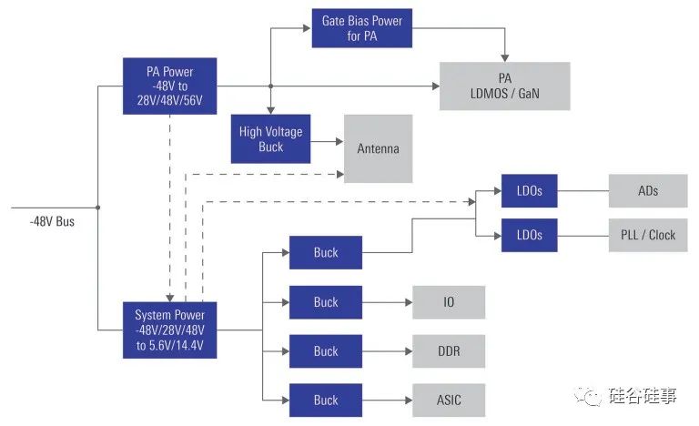
Figure 1, Typical 5G AAU power tree diagram (AC source not shown)
The detailed power architecture depends on site type, range coverage, location and distance from grid or remote power sources.
A previously-released48V bus power conversion reference design using the GaN FET approach came from one of the most well-known GaN FET companies, Efficient Power Conversion (EPC), the EPC9143 (seen in Figure 2). The entire design is open source2.
This reference design is based on an industry-standard 1/16th brick converter footprint and can convert from an input of 18V to 60V, and to an output of 12V rated at 25A, based on a two-phase interleaved configuration. In addition to the EPC GaN FETs, the design uses a 16-bit digital controller, running at 500kHz, and delivers peak efficiency of >95% (This controller has a DSP core and additional analog portion that for simplicity we’d call DSP in the article).
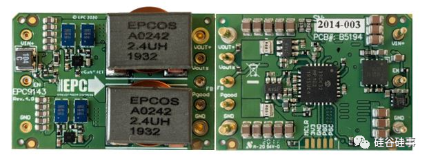
Figure 2 EPC9143 reference design with aDSP controller, top and bottom
While this design no doubt offers a very impressive performance, our team noticed it also uses six other integrated circuits (ICs), as seen in the Figure 2 reference design.
With many digital power controllers, users have the flexibility to re-program output voltage and protection thresholds, and may add other desirable features. However, for certain 48V applications, there is not as much need to re-program these configurations once a design is fixed, so the control modulator can be designed in an analog way as effectively as in digital. At Renesas, we started to think about whether we could combine and replace the seven ICs required in the EPC9143, with just one analog IC, and still achieve similar performance. While the DSP solution has nearly achieved the highest potential for GaN FET design with much greater efficiency than silicon FETs, achieving the same goal with simpler BOM would offer customers the benefits of higher power density and lower solution cost, which is as important as efficiency.
Following streamlined product definition, IC design and full validation work, Renesas developed an 80V dual synchronous buck controller specifically optimized to drive E-mode GaN FETs, the ISL81806 (Figure 3).
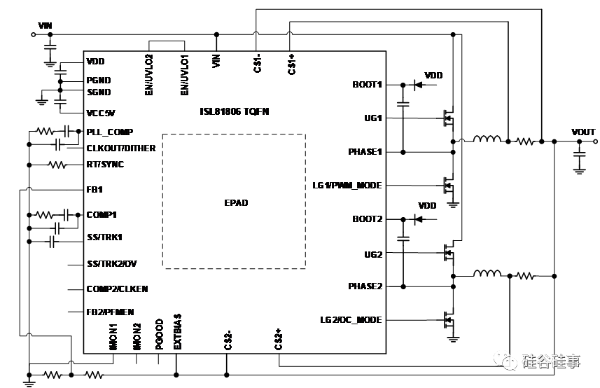
Figure 3 ISL81806 80V Dual output/TwoPhase GaN FET controller
The ISL81806 uses a two-phase interleaved topology and can be paralleled into up to six interleaved phases to take on kilowatt level load without the need for external digital control to distribute the phases.
Other features include:
Wide Vin range: 4.5V to 80V - allows telecom applications
Wide Vout range:0.8V to 76V
Support constant voltage or constant current output
Wide switching frequency: 100Khz to 2MHz
Diode emulation and burst mode at light load or forced PWM mode
Shoot-thru protection, OCP, OVP, OTP, UVP
Independent EN and soft start for each output
Gate drive and dead-time optimized for enhancement-mode GaN FETs
EPC and Renesas developed a new reference design board4 called EPC9157 (Figure 4). It is designed in the same two-phase interleaved topology and 1/16th brick module form factor as the DSP solution in Figure 2. The board is also rated at the same input voltage, output current, and same 500kHz frequency as the DSP solution. (At the time of this article’s release, this board can be rated to 80V input).

Figure 4: EPC9157 EVB using ISL81806 and four GaN FETs, analog control only
The efficiency of the DSP-based EVB and that of the analog-based EVB is shown as in Figure 5, and is quite close at peak power. The analog-based EVB has better light load efficiency, partially because one single analog controller consumes less operating current (50μA) than the seven combined ICs required in the DSP solution, and can directly use the 12V output as external bias for the IC supply.
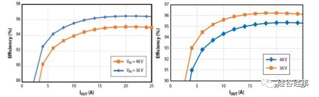
Figure 5 Efficiency Comparison (Left: EPC9143 using DSP, Right: EPC9157 using ISL81806)
Figure 6 below shows the key BOM differences between the digital and analog solutions (passive components omitted). It is very clear that the analog solution circuit BOM is incredibly simplified, requires only one IC, and does not require any programming.
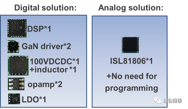
Figure 6 BOM difference
While ISL81806 already provides best-in-class efficiency, solution size and bill-of-material size, there is still room to improve in future revisions. Just as GaN FET technology has been rapidly evolving over the last few years, the team at Renesas working to define and design the matching controllers also faces new challenges and opportunities.
Some directions that future development may take us in include (but are not limited to):
Improved breakdown voltage
100V may be preferred for remote AAU as well as for board mount brick power modules, especially for telecom with long cables, in order to be more robust.
Stronger and separated gate drive
Stronger gate drivers may be desired for higher efficiency. However, this also brings very fast dV/dt, which has the potential to damage the IC with the negative voltage created by large stray inductance from any non-ideal layout. Separate turnon/off may be desired to optimize switching speed as in a discrete GaN driver IC like RAA226110 in reference 5.
Smallpackage for optimized layout
GaN suppliers recommend small packages like CSP or BGA without extended pins to further decrease systemstray inductance. However, certain applications with potential harsh environment deployment cannot accept CSP or BGA packages.
IC processimprovement
The IC switching node needs to be very robust to handle high dV/dt > 200V/ns and negative voltage during switching. The internal bootstrap diode may prefer near zero Qrr to enable high frequency. Such requirements may challenge the IDM or foundries to improve their IC manufacturing processes.
More studyinto the dead-time optimization
Having a little dead-time between the high-side switch turn off and the low-side switch turn on is required for safety purpose. During the dead-time, the “body-diode” function of the GaN FET conducts the load current. A GaN FET has a unique “body-diode”pattern with zero Qrr but a quite large forward drop6. Hence during dead-time, not only does the conduction loss increase, but the bootstrap capacitor may be overcharged to the point of damaging the top-side device. To optimize for a very small and still safe dead-time, we must also consider the IC and other BOM parametric shift due to temperature and mass production distribution. An E-MODE controller like the ISL81806 uses a fixed smallest dead-time optimized for GaN FETs, and the EPC9157 EVB is designed with external low-cost protection circuitry to avoid over-charging the bootstrap capacitor. However, this may have limited the practical operating frequency. Some DC/DC IC providers add a dead-time programming pin or make the dead-time digitally programmable. Eitherway, this leaves the hard job of dead-time selection to the circuit designers, and smarter IC features may be desired in the future. (Further reading can be found in reference 7 and 8.)
Add flexibility to adapt to various GaN technologies
Various GaNFETs, even all enhancement mode based, may have quite different designs, contrary to normal silicon FETs. For example, the recommended gate voltage can be quite different among manufacturers6 and become problematic as they need to be protected at different OVP levels. The gate drive voltage may need to be programmable, in addition to other possible variables in future offering.
GaN FETs have a bright future, and one day, they could be a “drop-in replacement” for silicon FETs with reasonable cost and much better performance, and controllers like the ISL81806 are helping to make that a reality with further product development to come. It is now as easy to use GaN FETs as to use silicon FETs when proper controllers are designed to control them.
References
1. TheEmerging 48V Ecosystem Power Electronics News 2019
https://www.powerelectronicsnews.com/the-emerging-48v-ecosystem%EF%BB%BF/
2. EPC9143
https://epc-co.com/epc/Portals/0/epc/documents/guides/EPC9143_qsg.pdf
3. https://upisemi.com/gan/
4. EPC9157
https://epc-co.com/epc/Portals/0/epc/documents/guides/EPC9157_qsg.pdf
5. RAA226110GaN driver product page
https://www.renesas.com/eu/en/products/power-power-management/fet-motor-drivers/gan-fet-drivers/raa226110-low-side-gan-fet-driver-programmable-source-current-and-adjustable-overcurrent-protection
6. Evaluationof Gate Drive Overvoltage Management Methods for Enhancement Mode GalliumNitride Transistors
David Reusch andMichael de Rooij 2017 IEEE APEC
7. GateDriver Design Guidelines for eGaN FETs
EfficientPower Conversion Corporation Presentation
8. Comparisonof deadtime effects on the performance of DC-DC converters with GaN FETs andsilicon MOSFETs
JohnS. Glaser and David Reusch
EfficientPower Conversion Corporation
