----追光逐电 光赢未来----

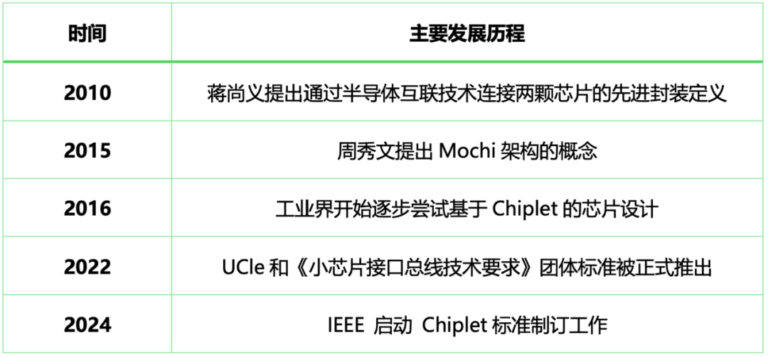
Chiplet的发展历程
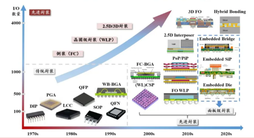
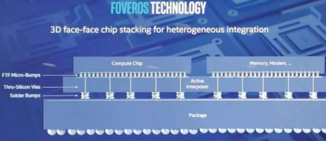
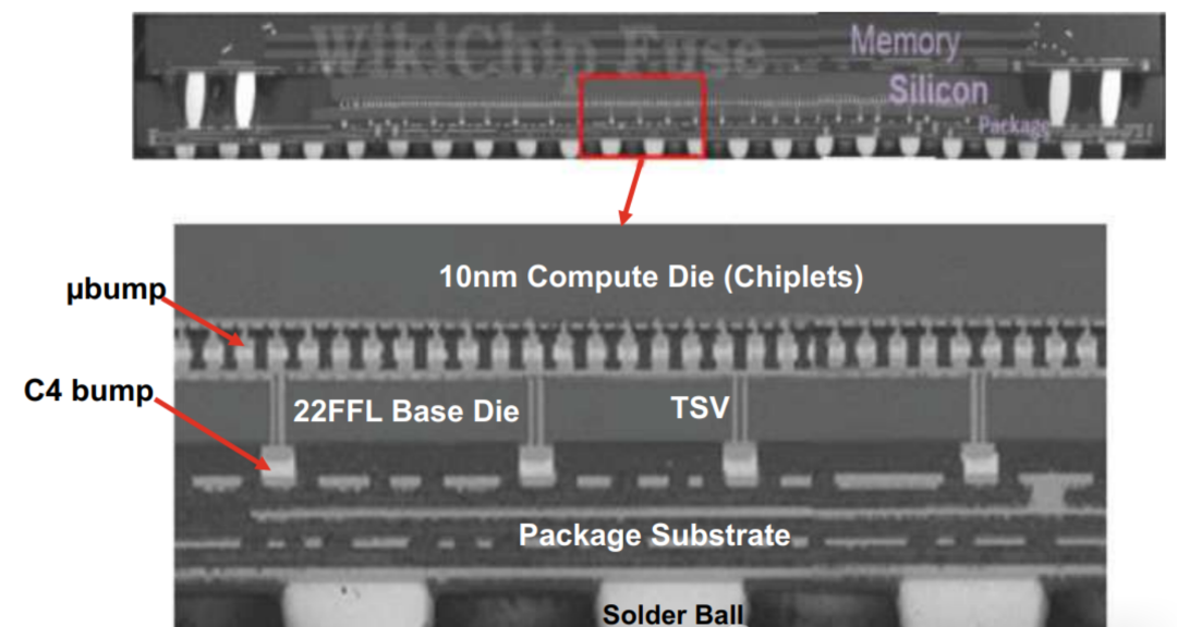
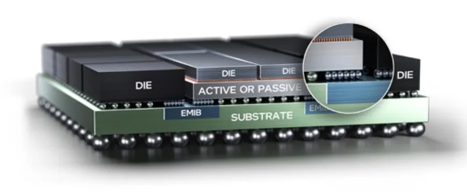
3.5D封装通过将逻辑芯片堆叠,并将它们分别粘合到其他组件共享的基板上,创造了一种新的架构。
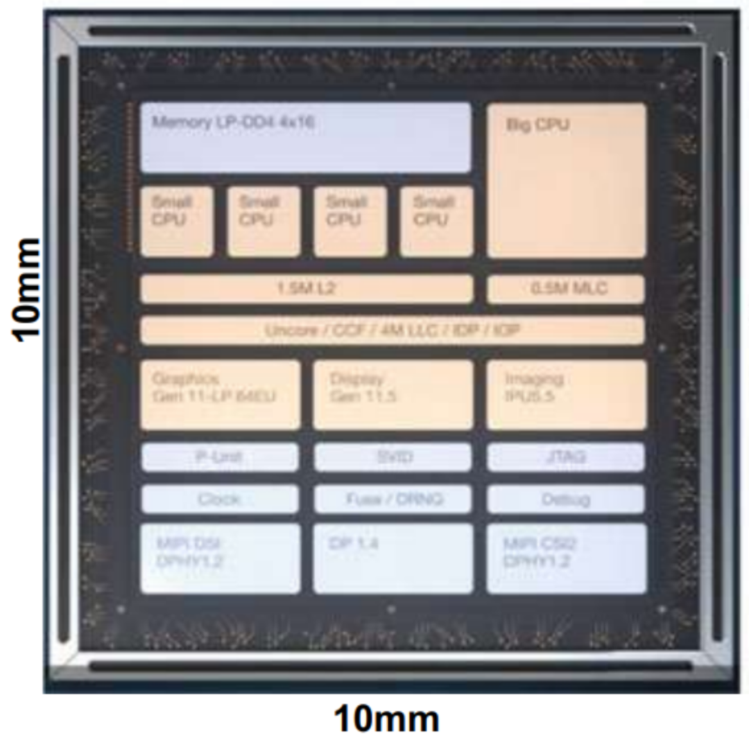
General AI computing chips can be built using high-bandwidth die-to-die chips (i.e., chiplet-to-chiplet) I/O, and then a large amount of DRAM bandwidth can be encapsulated to build an ideal LLM inference chip. Multiple AI chips can be packaged together as a high-end solution, or just one as a low-cost option. In all of these cases, once the initial chip has been created, the design and implementation costs are primarily in the package.
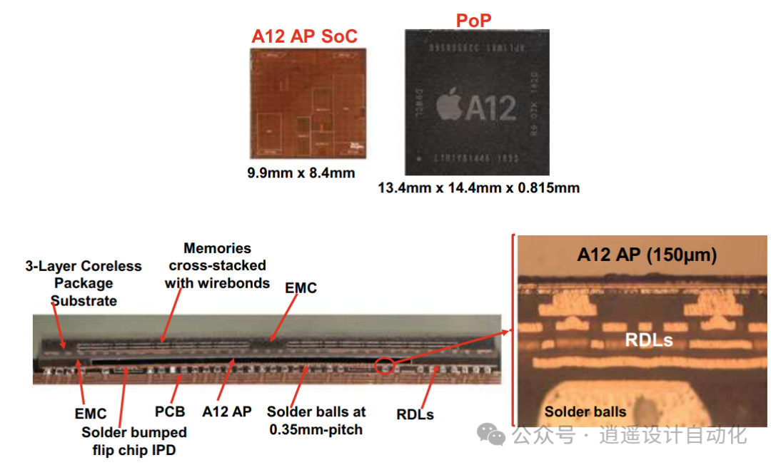
图8:苹果iPhone的PoP InFO Chiplet异构集成。
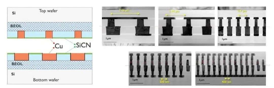
3.5D packaging creates a new architecture by stacking logic chips and bonding them separately to a substrate shared by other components.

申明:感谢原创作者的辛勤付出。本号转载的文章均会在文中注明,若遇到版权问题请联系我们处理。

----与智者为伍 为创新赋能----

联系邮箱:uestcwxd@126.com
QQ:493826566