IEEE国际存储研讨会(内存,闪存和新型存储技术)本周在韩国召开了!
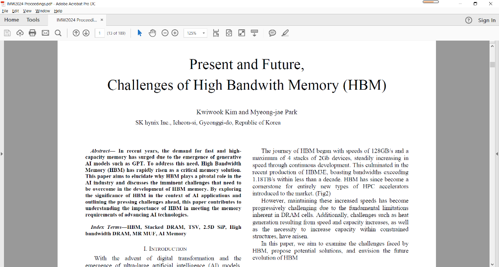
由 IEEE的Electron Devices Society (https://eds.ieee.org/)主办的IEEE International Memory Workshop 2024本周初在韩国首尔召开(5.12-5.15.2024)。其中SK Hynix将第一个做主旨发言,阐述HBM技术现在和未来面临的挑战,本次workshop也探讨了3D NAND进展和各种新型存储技术的最新研究,以及针对这些新型存储的仿真和测试技术。
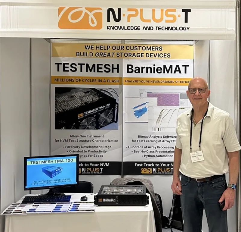
其中,意大利公司NplusT将在现场演示其针对NAND和各种新型存储的测试工具,同时在和韩国Samsung、SK Hynix进行技术交流后于下周(5.20 – 5.25)访问中国,计划与对于NAND和各种新型存储感兴趣的公司进行技术交流。感兴趣的朋友可以点击本文左下角的“阅读原文”获取下面的相关信息:
预约和NplusT测试技术专家Tamas Kerekes技术面对面交流
获得本次IMW2024活动论文/报告的详细图文介绍(pdf总计189页,58MB)
获得NAND测试工具的详细产品资料


本次IMW2024主旨讲演和报告内容一览:
Session 1: Keynotes
[1.1] Present and Future, Challenges of High Bandwith Memory (HBM)
[1.2] Exploring Innovative IGZO-Channel Based DRAM Cell Architectures and Key Technologies for Sub-10nm Node
[1.3] Flash Memory Revolution: Journey from 2D to 3D, Migrating to Modular Memory Fabrication
Session 2: NAND I
[2.1] Pure-Metal Replacement Gate for Reliable 30 nm Pitch Scaled 3D NAND Flash
[2.2] Novel Multi-Level Coding and Architecture Enabling Fast Random Access for Flash Memory
[2.3] 3D-NAND Based Filtering Cube with High Resolution 2D Query and Tunable Feature Length for Computational SSD
Session 3: Ferro/OTS/STT
[3.1] Engineering nvCap from FEOL to BEOL with Ferroelectric Small-Signal Non-Destructive Read
[3.2] AsSeGeS and GeN Heterostructures for Superior OTS Performance
[3.3] Novel Cross-Point Architecture Utilizing Distributed Diode Selector for Read Margin Amplification
[3.4] A Novel Test and Analysis Scheme to Elucidate Tail Bit Characteristics in STT-MRAM Arrays
Posters Session
[P1] Comprehensive Physics-Based Modeling of Post-Cycling Long-Term Data Retention in 176L 3-D NAND Flash Memories
[P2] Embedded Transformer Hetero-CiM: SRAM CiM for 4b Read/Write-MAC Self-Attention and MLC ReRAM CiM for 6b Read-MAC Linear&FC Layers
[P3] Modeling and Demonstration for Multi-Level Weight Conductance in Computational FeFET Memory Cell
[P4] Overcome the End of Life of 3D Flash Memory by Recovery Annealing, Aiming for Carbon Neutrality in Semiconductor Manufacturing
[P5] High-Efficient and Comprehensive Modeling of MFIM Ferroelectric Tunnel Junctions for Non-Volatile/Volatile Applications
[P6] SiGe/Si Heterojunction Drain Transistor for Faster 3D NAND FlashMemory Erase
[P7] Process Optimization and Cryogenic Evaluation of Spin-Orbit Torque Magnetic Random Access Memory
[P8] Realistic Noise-Aware Training as a Component of the Holistic ACiM Development Platform
[P9] A Novel Program-Verify Free and Low Drift Multi-Level Operation on Cross-Point OTS-PCM for In-Memory Computing Application
[P10] Optimizing RRAM Performance: A Comparative Analysis of Forming Strategies
[P11] Understanding the Thermal Aspects in Dense RRAM Memory Arrays
[P12] A 3.75Mb Embedded RRAM IP on 40nm High-Voltage CMOS Technology
[P13] High Operation Speed (10ns/100ns) and Low Read Current (sub-1μΑ) 2D Floating Gate Transistor
[P14] Role of Nitrogen in Suppressing Interfacial States Generation and Improving Endurance in Ferroelectric Field Effect Transistors
[P15] CMOS-Compatible Low-T Processing Methods for HZO-Based DRAM Capacitors by E-Field Cycling
Session 4: DRAM
[4.1] 3D X-DRAM: A Novel 3D NAND-Like DRAM Cell and TCAD Simulations
[4.2] Gate-All-Around SRAM: Performance Investigation and Optimization towards Vccmin Scaling
[4.3] Heterogeneous Oxide Semiconductor FETs Comprising Planar FET and Vertical Channel FETs Monolithically Stacked on Si CMOS, Enabling 1-Mbit 3D DRAM
[4.4] Multi-Gate Access Transistor to Minimize GIDL Leakage Current for Scaling
2-Tier Stacked 4F2 DRAM below Equivalent 10nm Node
Session 5: NAND II
[5.1] Demonstration of High-Growth-Rate Epitaxially Grown Si Channel on 3D
NAND Test Vehicle with Memory Functionality
[5.2] Modeling and Simulation for DRAM and Flash Memory Technology Exploration and Development
[5.3] Gate Side Injection Operating Mode for 3D NAND Flash Memories
[5.4] Design Framework for Ferroelectric Gate Stack Engineering of Vertical NAND Structures for Efficient TLC and QLC Operation
Session 6: Embedded & RRAM
[6.1] Charge Trapping Challenges of CMOS Embedded Complementary FeFETs
[6.2] Improvement of MAC Accuracy using Oxygen Diffusion Barriers in Resistive Synaptic Cell Arrays
[6.3] Self-Rectifying Non-Volatile Tunneling Synapse: Multiscale Modeling Augmented Development
[6.4] Performance and Reliability of Technology Qualified 34 Mb Split-Gate eFLASH Macro in 28 nm HKMG
Session 7: Ferro
[7.1] Materials Engineering for High Performance Ferroelectric Memory
[7.2] A Novel 3D Gate-All-Around Vertical FeFET with Back-Gate Structure for Disturbance-Less Program Operation
[7.3] Enhanced Reliability and Trapping Behavior in Ferroelectric FETs under Cryogenic Conditions
[7.4] Charge-Based Sense Demonstration in 1T-1C HZO FeRAM Arrays to Overcome CBL-Induced Bank Size Limitations
Session 8: 3D Processing
[8.1] Improved 3D DRAM Design Based on Gate-Controlled Thyristor Featuring
Two Asymmetrical Horizontal WL’s and Vertical BL for Better Cell Size Scaling and Array Selection
[8.2] D2W Hybrid Bonding Challenges for HBM
想了解更多关于NAND和新型存储测试技术,请添加saniffer公众号留言,或者致电
021-50807071 / 13127856862,sales@saniffer.com。
