
“To ensure the highest level of reliability in high RF power design applications, factors such as maximum device power, maximum voltage and current ratings, thermal characteristics of all circuit devices and various ways that heat is removed should be taken into account before being incorporated into the end product design.”
POWER DISSIPATION

The ESR takes into account all of the losses incurred by the dielectric material, electrodes, terminations and termination to electrode interfaces. It is interesting to note that capacitors that exhibit ultra-low ESR as well as high voltage breakdown characteristics (such as porcelain types) are especially well suited for high RF power applications.
A Capacitor Power Dissipation Example
Consider the following example consisting of a 51 pF RF porcelain chip coupling capacitor used in the power output stage of acellular base station operating at 900 MHz, as shown in Figure 1. The RF power is 60 W in a 50 W system; the coupling capacitor has an ESR of 0.061 W at 900 MHz. The total RF current in this application is determined using
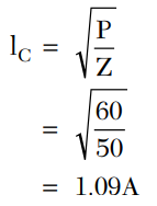
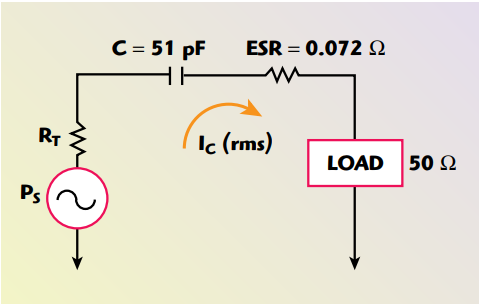
Fig. 1 Current flow through a capacitor with series loss element.
Therefore, the total power dissipated in the capacitor is

This example illustrates the importance of the relationship between ESR and the total power dissipated by the capacitor. Here, the power dissipated by the capacitor due to its internal losses represents 72 mW or 0.12 percent of the total power applied to the capacitor. This low loss is achieved by utilizing low ESR RF ceramic capacitors in these applications. Recent advances in materials technology have enabled the realization of lower ESR, further reducing the power dissipated by the capacitor.
CURRENT RATING
The maximum current rating assigned to a capacitor by the manufacturer is stated in one of two ways: voltage limited or power dissipation limited. The rating that applies depends on
the capacitance value and operating
frequency for a given application. If the
capacitor’s current rating (IC) in a particular application is limited by voltage
it can be calculated using the relationship between the rms voltage rating of
the capacitor and the capacitive reactance. Accordingly, the maximum current for the voltage limited operating
condition is directly proportional to the
capacitor rms voltage rating and inversely proportional to its reactance:
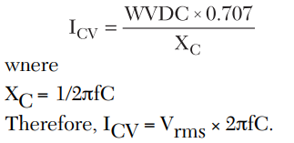
As the operating frequency or capacitance is increased, a region on the current curve is entered where the numerical value of the voltage limited current is equal to that of the current limited by power dissipation. This condition occurs at the intersection of the dotted and solid lines as shown in Figure 2. At frequencies above this intersection point the current rating is determined solely by the power dissipation limit. In this region the maximum current is calculated using

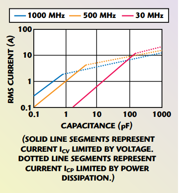
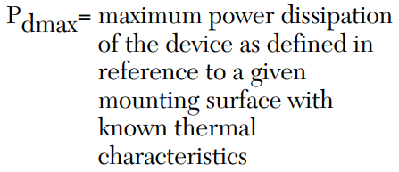
Hence, in this region the maximum current is now limited by the capacitor’s power dissipation limit. Regardless of the specified power rating (a somewhat relative term), a capacitor exhibiting low ESR is always desirable for providing an optimum device current rating.
VOLTAGE RATING
Maximum voltage ratings are determined predominantly by the dielectric strength or voltage breakdown characteristics of the dielectric material. As an example, porcelain dielectrics exhibit a breakdown voltage that typically exceeds 1000 V/mil of dielectric thickness and is virtually constant over the specified operating temperature range. Other dielectrics fabricated from barium titaniate (BaTiO3) based materials for example will exhibit lower breakdown voltage characteristics due to differences in their chemical and microstructural compositions, as shown in Figure 3.
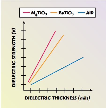
Fig. 3 Voltage vs. dielectric thickness
A voltage breakdown also may occur on the outside of the device package. In this instance, the applied voltage is large enough compared to the length of the external path (termination to termination) in air to produce a flashover. Other factors that may promote an external breakdown are surface contamination as well as environmental factors such as humidity and sharp edges, especially in the immediate areas of the terminations. One method of testing for dielectric strength is to submerse the test sample in an insulating oil bath, thereby eliminating the incidence of external flashover failure.
THERMAL RESISTANCE
The thermal resistance of a ceramic capacitor operating in a given application is a key factor that must be
known in order to establish the de- vice power rating Pdmax. Knowing
the length of the heat flow path, the
thermal gradient and the perpendicular area, as shown in Figure 4, makes
it possible to determine the thermal
resistance θ.
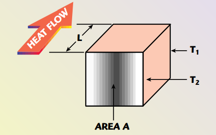
Fig. 4 Heat flow path, thermal gradient and termination area of a ceramic capacitor
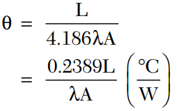
The thermal resistance for a given capacitor structure with length L and cross-sectional area A can be expressed by the relationship
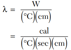
Thermal conductance λ is expressed as
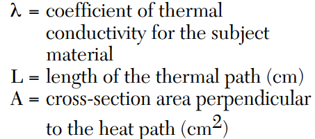
where
Note that multiplying [W/(°C)(cm)] by 0.2389 converts the units to cal/(°C)(sec)(cm). In addition, the thermal conductivity λ is essentially constant over the normal temperature range of 25° to 125°C.
From this expression it can be readily seen that the thermal resistance is proportional to the length of the heat flow path and inversely proportional to the thermal conductivity and the crosssectional area perpendicular to the heat flow path. This relationship suggests that the aspect ratio of the capacitor, that is, the ratio between width and length, plays an important role in the determination of the thermal resistance. The power dissipation of the device can be determined from the thermal resistance expression by establishing the temperature differential across the heat flow path and dividing by θ. Hence, the maximum power dissipation is expressed as
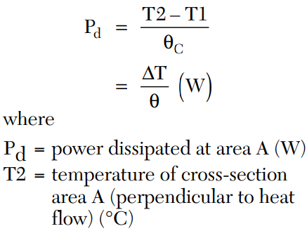
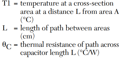
The thermal model used for calculating the maximum power dissipation of a ceramic capacitor typically takes into account the thermal resistance of the capacitor and its mounting surface. This model assumes that heat is removed mainly by conduction through the capacitor’s terminations and external leads. Since heat removal by radiation and convection is disregarded in this model, a safety factor for maximum power dissipation therefore is established. The model further assumes that the thermal resistance of the capacitor’s terminations is insignificant compared to the ceramic body and, hence, is disregarded. The effects of the mounting surface also are disregarded and an infinite heat sink is assumed for the temperature rise calculation shown in Figure 5.
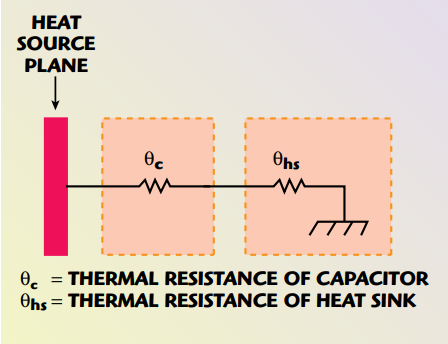
Fig. 5 The thermal model of a capacitor mounted on a heat sink.
TEMPERATURE RISE
The maximum change in temperature along the heat flow axis is referred to as the temperature rise or thermal gradient. The hypothetical determination of temperature rise as a function of RF current is not always straightforward. To get a reasonable handle on this value the designer must account for the ESR and thermal resistance of the capacitor as well as its mounting surface.
Given the ESR and current in an application, the capacitor’s power dissipation PCD as well as the heat generated in the capacitor can be calculated. The thermal resistance of the capacitor and its external connections to a heat sink also can be ascertained and, hence, the temperature rise above the ambient can be established. Assuming an infinite heat sink and a capacitor with zero manufacturing flaws, the temperature rise can be calculated using
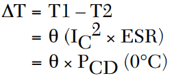
Figure 6 shows the relationship between the capacitor’s power dissipation and the change in the capacitor’s case temperature.
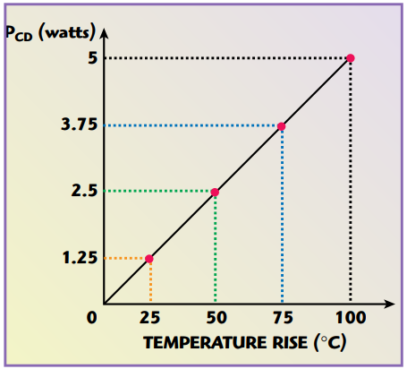
Fig. 6 PCD as a function of temperature.
HEAT TRANSFER METHODS
Heat may transfer either to or from the boundaries of a ceramic capacitor structure in several ways. Heat transfer occurs only when a temperature difference exists between the capacitor and its immediate surroundings. Heat is transferred by conduction, convection and radiation, which may occur separately or in combination.
Thermal Conduction
Heat energy transferred by conduction takes place in ceramic capacitor structures essentially at the termination areas. In this case, heat transfer takes place because there is physical contact between the capacitor terminations and the points of connection on the board surface. Energy transfer by conduction occurs in the direction of decreasing temperature and is due to the temperature gradient along the length of the heat flow path.
On the molecular level, conduction can be thought of as the transfer of energy from a more energetic thermal state to a less energetic thermal state. Therefore, as molecules collide with each other energy is transferred in the form of heat from the more energetic to the less energetic molecules. This heat transfer is due to the random movement of molecules and the interactions between them within the two thermal gradients. As the temperature increases, the activity or interaction between the molecules also increases. These molecules collide with each other and, hence, transfer energy in the form of heat.
From Fourier’s law of heat conduction the conduction process can be quantified as a heat flux rate equation. The law states that the rate of heat flow through a solid homogeneous structure is directly proportional to the area of a section at right angles to the direction of heat flow path and to temperature differences per unit length along the path of heat flow, as shown in Figure 7. Thus,
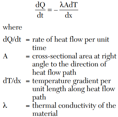
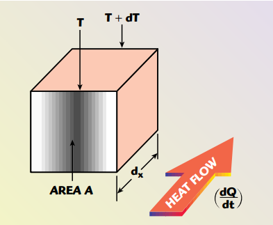
Fig. 7 Heat flow through a solid homogeneous structure.
Note that the negative sign associated with λ indicates that the heat flows conductively from high to low temperatures, or against the temperature gradient.
Thermal Convection
Energy transfer between a solid surface and moving air in the immediate surroundings is commonly referred to as convection. The heat transfer due to convection is an interactive combination of diffusion or molecular motion in the dielectric material and the bulk movement of the surrounding air. There are basically two types of convection heat transfers: natural (free) and forced. Natural convection currents are induced by forces due to differences in variations between the device surface temperature and the surrounding ambient temperature; that is, heat is directly picked up by the air and transported away. Natural or free convection is caused by air movement due to thermal gradients between an object (in this case a ceramic capacitor) and its surrounding ambient environment.
Forced convection heat flow is induced by external means, such as a cooling fan. Heat transfer coefficients due to forced flow are generally greater than that of natural convection flow. In most cases the free convection may be neglected when there is forced airflow, hence forced convection provides the greater effect for convection cooling.
Newton’s law of cooling is used to model the temperature change of an object that is at some initial elevated temperature placed in an environment of a lower temperature. The law states that the rate at which a warm body cools is approximately proportional to the temperature difference between the temperature of the warm object and the temperature of its immediate surroundings. Thus,
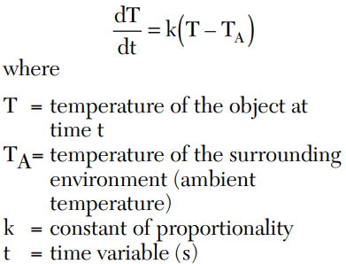
Solving the differential equation for T means placing T on one side and t on the other, such that

Integrating both sides produces

and solving for T gives

From this expression it can be seen that the cooling process is exponential, that is, rapid at first, then levels off. Hence, this characteristic may be thought of as the thermal time constant of an object. The temperature of the object T now can be directly expressed at time t (s). In Newton’s law of cooling, t is the variable where TA, k and C are constants. In order to determine the temperature of the object at a given time, all of the constants must have numerical values.
Thermal Radiation
Thermal radiation is energy emitted by matter and transported by electromagnetic waves or photons. While the transfer of energy by convection or conduction requires the presence of a medium, electromagnetic waves do not require a medium to propagate and will transfer heat energy most efficiently in a vacuum. The total energy at which radiation may be emitted from a surface as photons per second by a square centimeter of an ideal black body radiator is equal to the temperature raised to the fourth power. This energy emission results from changes in the electron configurations of the atoms or molecules of the radiating object.
Stefan-Boltzmann’s law gives the maximum heat flux at which radiation may be emitted from a surface. The law takes the form
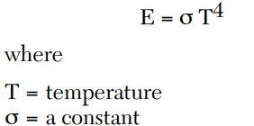
From this equation it can be seen that a small increase in temperature produces a very large increase in emitted radiation energy. If the temperature is doubled, the energy emitted increases by a factor of 16. The surface emissivity indicates how efficiently the surface of a given object will emit radiation energy relative to an ideal black body radiator. The ideal black body has an emissivity reference equal to 1.0. Just as surfaces emit energy, another surface can absorb a portion of that energy. The surface properties of various materials will affect the amount of heat radiated.
The intensity of radiation is defined as the rate of emitted energy per unit of surface area through a unit solid angle. The radiation from a surface has different intensities in different directions. The intensity of radiation along the normal to the surface is known as the intensity of normal radiation.
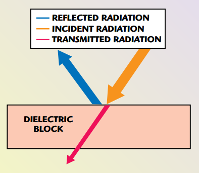
When thermal radiation strikes a solid object, portions of the energy can be absorbed, reflected or transmitted through the object. This energy is dispersed in various proportions depending on the surface emissivity and density of the material, as shown in Figure 8. The portion of the incident radiation that is absorbed by the object is its absorptivity α. Another portion of the incident radiation energy will be reflected and is referred to as reflectivity ρ. Lastly, the portion of the radiated energy that is transmitted though the object is referred to as transmissivity τ. The sum of all of these portions of the radiated energy is unity and, therefore,


Fig. 8 Thermal radiation dispersion.
APPLICATION CONSIDERATIONS
This article has highlighted several major factors to consider while designing circuit elements for high RF power applications. Some of the most important considerations relate directly to such things as ESR, thermal resistance of the device(s), mounting surface characteristics and heat removal. These factors are associated with the overall thermal management of the entire design and should necessitate careful assessment of all circuit elements and their contribution to the overall thermal load on the design. Some of the guidelines for these considerations are summarized below.
• It is always prudent to select capacitor products with ultra-low ESR and dissipation factor characteristics, especially concerning thermal management considerations of high RF power designs. This choice will ensure the most efficient operation and minimize the amount of heat generated in the application.
• The thermal resistance of the capacitor’s mounting surface and heat sink should be as low as possible. Since the heat is primarily conducted by the capacitor’s terminations to the metallic contact points on the board, it is important to evaluate characteristics such as thermal conductivity of all materials involved as well as board trace dimensions and material thickness at the points of contact.
• Since the greater part of the heat transfer is predominantly through the terminations of the capacitor, the thermal path of a ceramic chip capacitor may be further improved by the use of external leads such as silver microstrip ribbon. The ribbon leads will serve to bleed heat away from the capacitor more efficiently. The leads also may serve as a mechanical strain relief, especially in situations where the coefficient of thermal expansion between the capacitor and the board material is significantly mismatched. The silver lead stock is tailored to the width of the capacitor body, making it suitable for this purpose.
• The overall thermal management of the entire design must be judiciously evaluated. Devices such as power FETs and active gain blocks as well as other passives in an application will provide additional sources of heat during operation and thereby add to the overall thermal load of the design module. Care must be taken to account for the impact of all of the heat sources in the final design.
• Using capacitor assemblies that employ several capacitors in parallel will serve to greatly extend the current and power rating over a single capacitor. Assemblies that utilize ruggedized porcelain capacitor building blocks in various combinations will greatly extend the capacitance, voltage and current handling capabilities. For example, two equal value capacitors in parallel will yield approximately one-half the ESR of one capacitor and thereby afford virtually twice the current handling capability, an advantage that is difficult to ignore.
CONCLUSION
To ensure the highest level of reliability in high RF power design applications, factors such as maximum device power, maximum voltage and current ratings, thermal characteristics of all circuit devices and various ways that heat is removed should be taken into account before being incorporated into the end product design. In addition, when selecting ceramic chip capacitors for these applications it is prudent to first evaluate the ESR of the particular capacitor(s) at the application operating frequency. Knowing the ESR along with the network impedance will allow the designer to perform quick calculations of the power dissipated by the capacitor. This consideration is equally important for all other circuit elements in the application. Proper design with emphasis on thermal management will help to ensure efficient and troublefree operation.
声明:
投稿/招聘/推广/宣传 请加微信:15989459034
