APPLICATIONS FOR RF TRANSFORMERS
RF transformers are widely used in electronic circuits for
Impedance matching to achieve maximum power transfer and to suppress undesired signal reflection.
C Voltage, current step-up or step-down.
C DC isolation between circuits while affording efficient AC transmission.
C Interfacing between balanced and unbalanced circuits; example: balanced amplifiers.
TRANSFORMER CIRCUITS AND IMPEDANCE RELATIONSHIPS
When signal current goes through the primary winding, it generates a magnetic field which induces a voltage across the secondary winding. Connecting a load to the secondary causes an AC current to flow in the load.
It is generally necessary to control terminating impedances of RF signal paths, especially in wideband applications where path lengths are not negligible relative to wavelength. Wideband RF transformers are wound using twisted wires which behave as transmission lines, and the required coupling occurs along the length of these lines as well as magnetically via the core. Optimum performance is achieved when primary and secondary windings are connected to resistive terminating impedances for which the transformer is designed. Transformers having a turns ratio of 1:1, for example, are typically designed for use in a 50- or 75-ohm system.
In this application note, reference is continually made to terminating impedances which the user should provide for transformers, both for performance testing and in actual use. For the sake of consistency in the discussion, transformers with turns ratio greater than 1:1 will be described as step-up; that is, the secondary impedance is greater than the primary impedance. In actual use, however, connection can be step-up or step-down as needed.
V2 = N V1 and I2 = I1 / N, where N is the turns ratio.
Since Z2 = V2 / I2 and Z1 = V1 / I1, Z2 = N2 Z1. That is, the impedance ratio is the square of the turns ratio.
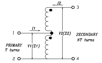
Figure 1a Autotransformer
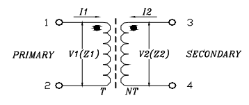
Figure 1b Transformer with DC Isolation
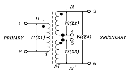
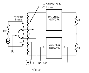
In the equations for Figure 1c which follow, the turns ratio N refers to the entire secondary winding.
V4 = N V1, and V2 = V3 = N V1 / 2
When the two halves of the secondary are connected to equal terminating impedances Z2 and Z3 , then
I2 = I3 = I1 / N; Z4 = N2 Z1 , and Z2 = Z3 = Z4 / 2 = N2 Z1 / 2
A variation on the transformer of Figure 1c, favoring high frequency performance, is shown in Figure 2. It adds a transmission-line transformer in cascade at the input, to convert an unbalanced signal to balance at the input to the center-tapped transformer. Features of this design:
Wide bandwidth, exceeding 1000 MHz.
Excellent amplitude and phase balance.
Higher return loss (lower VSWR) at the primary side.
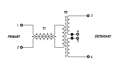
Figure 2 High-frequency Transformer with Balun on Primary Side
TRANSFORMER PERFORMANCE CHARACTERISTICS
Insertion Loss and Frequency Bandwidth
Insertion loss of a transformer is the fraction of input power lost when the transformer is inserted into an impedance-matched transmission system in place of an ideal (theoretically lossless) transformer having the same turns ratio. Actual insertion loss is affected by non-ideal characteristic impedance of the transformer windings, as well as winding and core losses.
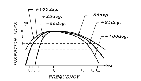
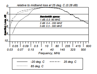
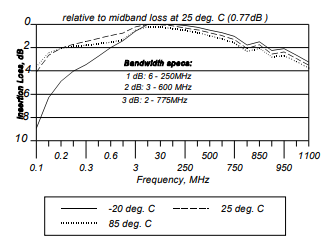
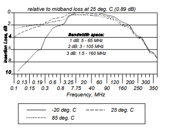
Typical insertion loss variation with frequency is illustrated in Figure 3 which shows the 1 dB, 2 dB, and 3 dB bandwidths, referenced to the midband loss as they are usually specified. Insertion loss at low frequency is affected by the parallel (magnetizing) inductance. At low temperature, low-frequency insertion loss tends to increase because of decreasing permeability of the magnetic core. High-frequency insertion loss is attributed to interwinding capacitance, series (leakage) inductance, and core and conductor losses. At high temperature it tends to become greater due to increase in the loss component of core permeability.
A further influence on transformer insertion loss is high AC or DC current. Most RF transformers are used in small-signal applications, in which typically up to 250 mW of RF or 30 mA of unbalanced DC current pass through the windings. In the interest of small size and widest bandwidth, the smallest practical size of cores is used. When insertion loss specifications must be met with greater RF power or DC current applied, this must be taken into account in the transformer design to prevent saturation of the magnetic core and consequent bandwidth reduction.
How is insertion loss of a transformer measured? This question is especially pertinent for impedance ratios other than 1:1 because accommodation must be made for the impedance of test instrumentation, which is generally a constant 50 or 75 ohms. There are three methods:
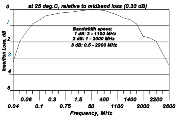
Actual midband insertion loss is noted above each graph.
Impedance and Return Loss
Impedance looking into the secondary winding is measured with the primary winding terminated in its specified impedance (usually 50 or 75 ohms), and compared with the theoretical terminating value (Z1 , Z2 , or Z3 in Figure 1).
Return loss, or VSWR, is measured at the primary winding, with the secondary terminated in its theoretical impedance; e.g., 2 x Zprimary for a 1:2 impedance-ratio (1:1.414 turns-ratio) primary transformer.
PHYSICAL PARAMETERS OF A TRANSFORMER
The performance of RF transformers can be understood with the help of the equivalent circuit in Figure 8
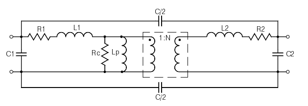
L1 and L2 are the primary and secondary leakage inductances, caused by incomplete magnetic coupling between the two windings. Because their reactance is proportional to frequency, these inductances increase insertion loss and reduce return loss at high frequency.
R1 and R2 are the resistance, or copper loss, of the primary and secondary windings. Skin effect increases the resistance at high frequencies, contributing to the increase in insertion loss.
Intra-winding capacitances C and C , as well as interwinding capacitance C, also contribute 1 2 to performance limitations at high frequency. However, the distinct advantage of the transmission line design used in RF transformers is that much of the interwinding capacitance is absorbed into the transmission line parameters together with the leakage inductance (parallel capacitance and series inductance), resulting in much wider bandwidth than is obtainable with conventional transformer windings.
Lp is the magnetizing inductance, which limits the low frequency performance of the p transformer. It is determined by the permeability and cross-sectional area of the magnetic core, and by the number of turns. Insertion loss increases and return loss decreases at low frequency. Further, permeability of many core materials decreases with a decrease in temperature and increases above room temperature. This accounts for the spread of the lower frequency portion of the insertion loss curves in Figure 3 as explained above.
Temperature variation of the capacitances and the leakage inductances is relatively small. The winding resistances do vary, increasing with temperature, and contribute to the spread of the high frequency portion of the curves in Figure 3.
The resistance Rc represents core loss. There are generally three contributions to this loss:
C eddy-current loss, which increases with frequency
C hysteresis loss, which increases with flux density (applied signal level)
C residual loss, due partially to gyromagnetic resonance
MEASUREMENT OF AMPLITUDE AND PHASE BALANCE: CENTER-TAPPED TRANSFORMERS
Definitions
Amplitude balance, sometimes called "unbalance", is the absolute value of the difference in signal amplitude, in dB, between the two outputs of a center-tapped transformer using the center tap as a ground reference.
Phase balance, sometimes called "unbalance", is the absolute value of the difference in signal phase between the two outputs of a center-tapped transformer using the center tap as a ground reference, after subtracting the 180-degree nominal value of the phase-split.
Measurement Method: Matching Network Between Each Half of the Transformer Secondary and Sensing Port in the Test Instrumentation
It was mentioned above, toward the end of the section on insertion loss measurement, that a transformer having a center-tapped secondary can be tested like a power splitter. There is a difference which must be considered, however: A device built as a power splitter has an internal circuit which provides isolation between the outputs; that provision ensures constant impedance looking into each output port independent of the load on the other output. A transformer on the other hand, being a simpler device, lacks isolation. Thus, the design of the matching network must take into account not only the primary source impedance transformed by the primary-to-half-secondary ratio, but another impedance in parallel with it: the input impedance of whatever is terminating the other half-secondary winding.
The situation is illustrated in Figure 9. R is the source and sensing port impedance of the test t instrumentation, as well as the impedance for which the primary of the transformer is designed. The total secondary must be terminated in N2Rt. Therefore, each of the matching 2 t networks, while its output is terminated in Rt, must have an input impedance N2R1 / 2.
The output source impedance of each matching network, because it has to feed a cable presenting a load Rt, must also equal Rt. This must be while the matching network is being fed from a source impedance which is the parallel combination of two impedances as follows: One is the transformed source impedance R which appears at the half-secondary as (N / 2)2Rt. The other is the input of the other matching network, N2Rt / 2, coupled from one half-secondary to the other. The resultant is N2 Rt / 6.
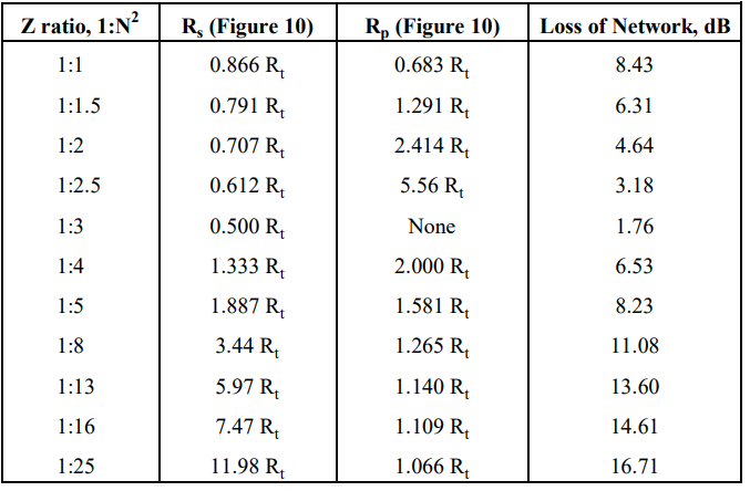
The impedance constraints for the matching network require three topologies depending upon the value of the transformer impedance ratio N2, as shown in Figures 10a through 10c.
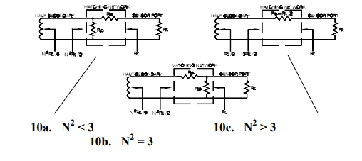
For each of the two non-trivial cases, 10a and 10c, the requirements for input and output impedance to the network provide two equations to solve for the two unknowns Rs and Rp. For N2 < 3, referring to Figure 10a, the equations are:
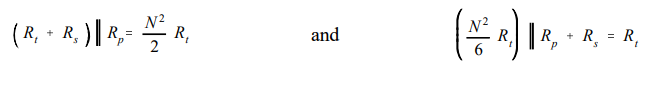
 For N2 > 3, referring to Figure 10c, the equations are:
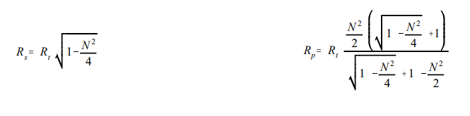
The solution is:
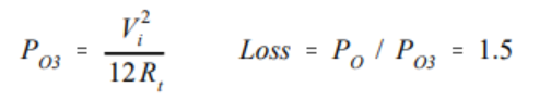
For N2 = 3, Rs = Rt / 2 and Rp is infinite.
For accurate RF phase balance measurement, the construction of the matching networks and the connections to them should be such as to provide electrical symmetry between the two halves of the circuit.
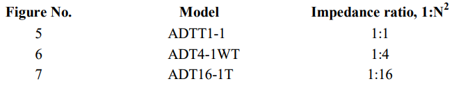
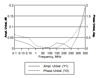
To show the effectiveness of the above method, it was used to test transformers for amplitude and phase unbalance, with results shown in Figures 11, 12, and 13. These are the same transformers for which insertion loss was given in Figures 5, 6, and 7.
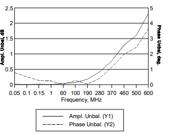
Figure 11 Model ADTT1-1 Amplitude, Phase Unbalance
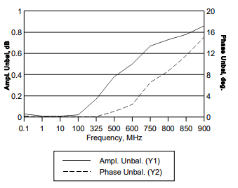
Figure 12 Model ADT4-1WT Amplitude, Phase Unbalance
The remaining task is to derive expressions for the insertion loss of the matching network, so that it can be subtracted from measured values to yield insertion loss for the center-tapped transformer itself when it is tested by the "power splitter" method described above. As a reminder, 3 dB (for the split) must also be subtracted from the measured values.
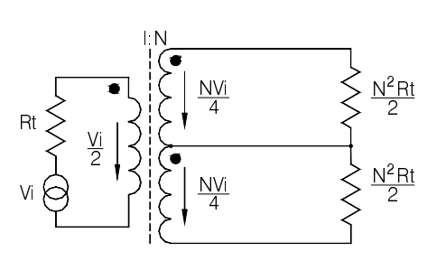
Figure 14 shows voltage relationships for a transformer with the secondary terminated in matched resistive impedances.
The voltage across the primary is half the open-circuit source voltage V , because the i impedance looking into the primary is R . The power delivered to each terminating resistor is t the square of the voltage divided by the resistance:
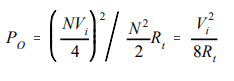
Figure 15 shows what happens when the various matching networks are inserted after the half-secondary, and the matched load per Figure 10 is replaced by R which represents the t sensor port in the instrumentation.
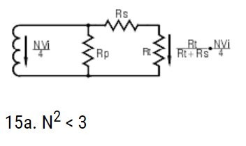
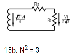
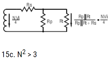
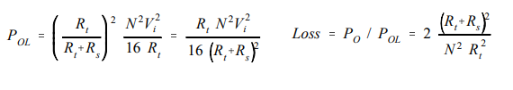
Figure 15b illustrates the N2 = 3 case per Figure 10b:
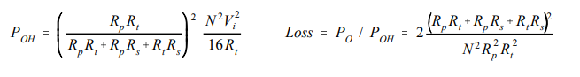
Resistors available for the matching networks are typically the "1% values". Their nominal values, having increments of 2%, could thus differ from the Table 1 values of R and R by s p as much as ± 1%. The resulting error in the loss of the network is greatest if R and R depart s p from Table 1 in opposite directions, and amounts to 0.1 dB for N2 = 5, for example, in the case of 1% resistance error. If greater accuracy is needed, loss should be calculated by substituting the actual resistances in the equations following Figure 15.
来源:Mini-Circuits

声明:
投稿/招聘/推广/宣传 请加微信:15989459034