图文导读
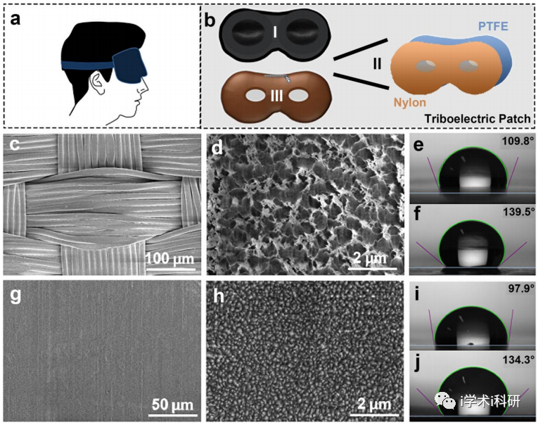
Figure 1. (a) Simulated diagram of the triboelectric patch. (b) Schematic diagram of the triboelectric patch components. (c) Scanning electron microscope image of the ICP-etched nylon fabric. (d) Magnification of the image in panel c. (e, f) Profiles of a water drop on (e) untreated and (f) ICP-etched nylon fabric. (g) Scanning electron microscope image of the ICP-etched PTFE. (h) Magnification of the image in panel g. (i, j) Profile of a water drop on (i) untreated and (j) ICP-etched PTFE.
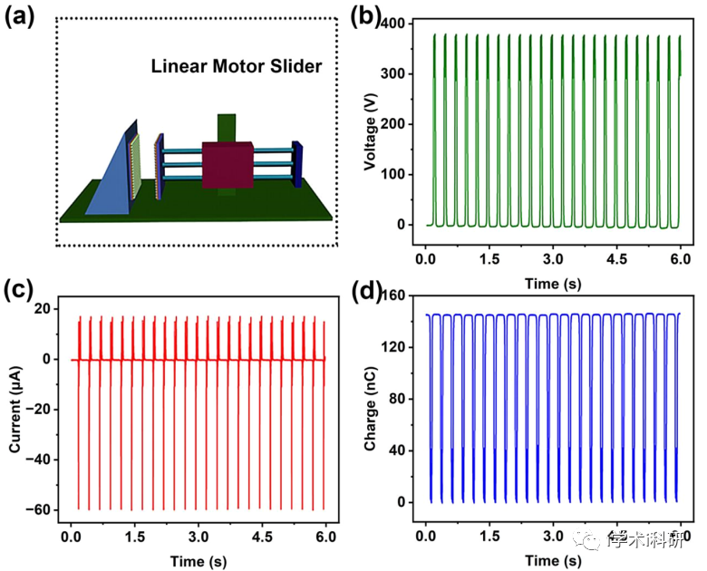
Figure 2. (a) Schematic illustration of the measurement for electrical performance tests and (b) Voc, (c) short-circuit current (Jsc) and (d) transferred charges.
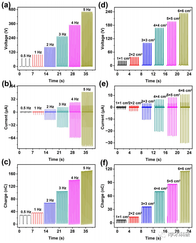
Figure 3. Electrical outputs of the designed TENG with surface area of 4 cm × 4 cm at various motion frequencies (0.5−5 Hz).
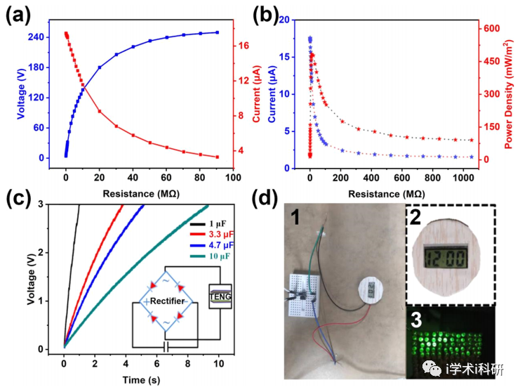
Figure 4. (a) Maximum output voltage and current versus different load resistances. (b) Dependence of Jsc and output power on external load resistance driven by the designed TENG. (c) Capacitor charging for 1, 3.3, 4.7, and 10 μF capacitor using the designed TENG. (d1) Powering of digital watch using 10 μF capacitor; (d2) enlarged photograph of the working digital watch; (d3) photograph of an LED lighting panel driven by the designed TENG.
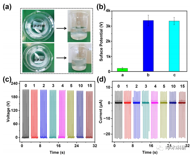
Figure 5. Washing durability tests of our designed TENG.
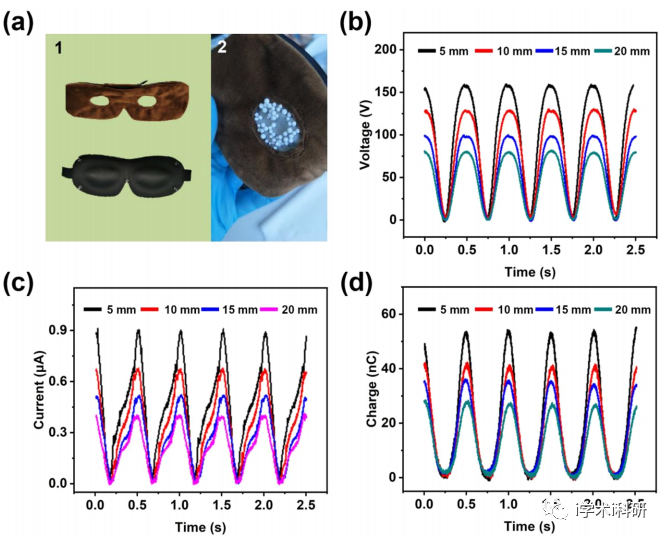
Figure 6. (a) Optical images of triboelectric patch components. Electrical output characterization of the as-fabricated electrodeless TENG with collectors: (b) Voc,(c) Jsc, and (d) short-circuit transfer charge of the designed electrodeless TENG.
