中国最活跃的射频微波天线雷达微信技术群
电子猎头:帮助电子工程师实现人生价值!
电子元器件:价格比您现有供应商最少降低10%
射频微波天线新产品新技术发布平台:让更多优秀的国产射频微波产品得到最好的宣传!发布产品欢迎联系管理,专刊发布!强力曝光!

作者:QING-QIANG HE1 , SHUAI DING 2 , CHEN XING1 , JUN-QUAN CHEN1 , GUO-QING YANG1 , AND BING-ZHONG WANG 2 , (Senior Member, IEEE)
Structurally integrated antenna is a kind of highly integrated microwave device with a load-bearing function,and it is usually installed on the structural surface of the air, water and ground vehicles. This paper presents the design, fabrication and testing of a novel structurally integrated Ka-band active antenna for airborne 5G wireless communications. The proposed antenna is mainly composed of three parts: a package layer, a control and signal process layer and a RF layer. In the RF layer, the microstrip antenna array, tile transmitting (Tx) modules, micro-channel heat sinks and a stripline feeding network are highly integrated into a functional block with a thickness of 2.8 mm. Electromechanical co-design methods are developed to design the active antenna array with the superstrates, and two schemes for designing micro-channel heat sinks are evaluated to obtain a uniform temperature distribution. The RF layer is fabricated by using the low-temperature cofired ceramic process, and the three layers are assembled to form the full-size antenna prototype. The mechanical and electromagnetic experiments are carried out, and the results demonstrate the feasibility of the structurally integrated active antenna for airborne wireless communications.
Significant momentum has started to build around the 5G wireless communication technologies for delivering mobile experience differentiation by providing higher data rates, lower latency, and improved link robustness . In this regard, millimeter-wave phased array antenna is a very promising solution for 5G wireless communications, due to the wide bandwidths and steerable beams. The millimeter-wave phased array antenna can be applied to realize the wireless connection between the base stations and wireless terminals in a mobile vehicle such as the aircraft, high-speed train, car, and ship. Moreover, it can be continuously steered to the base stations, which could guarantee reliable connec-tions in these mobile environments . In addition, the multi-gigabits-per-second data speeds in 5G will provide new wireless communication applications such as uncompressed video streaming, mobile distributed computing, fast large file transfer, and office in a high-speed mobile environment. However, because of the limited space in a mobile vehicle like the aircraft, the phased array antenna is usually required to have a compact size, light weight and easy installation. In this condition, it is highly desirable to use structurally integrated active antennas for 5G wireless communications in a mobile vehicle.
Structurally integrated active antennas can embed an active planar printed antenna into the structural surface of the aircraft, high-speed train, car, ship, and armored vehi-cles. For example, the active microstrip antenna array is integrated into the wing or fuselage of an aircraft. Compared with the antennas mounted on the structural sur-face, structurally integrated active antenna features several advantages such as reduced weight, volume and aerodynamic drag.Structurally integrated active antenna is a kind of highly integrated antenna, which receives great attention in recent years. Antenna-on-chip (AoC) and antenna-in package (AiP) solutions are two commonly used techniques to realize the highly integrated antennas . Compared to AiP, AoC solutions eliminate the need of off-chip connections between dies and antennas,but reduce the reliability on manufacturing precision. Low-temperature cofired ceramics (LTCC) and liquid crystal polymer (LCP) are two very attractive materials for fabricating the AiP, and the mainstream SiGe or CMOS technologies are usually adopted to fabricate the AoC , the authors conducted a chronological review of the research on the AiPs using the LTCC, and the AiPs applied to realize the millimeter-wave communication were demonstrated in. LCP is also a competitive substrate and packaging material due to its excellent electrical properties, flexibility, and multi-layer lamination capability. Several researchers have utilized the LCP to fabricate the AiP and demonstrated wideband, high-gain, and high-efficiency antenna applications . All of the studies promote the development of highly integrated antennas. However, most of the previous studies concentrate on the antenna technology, interconnect and package pro-cesses, while the heat dissipation of the highly integrated active antennas is not considered. Besides, the AiP and AoC cannot be directly installed on the structural surface of the air-craft, high-speed train, car, ship, and armored vehicles, due to the lack of the load-bearing function. Different from the AiP and AoC, this work proposes a structurally integrated active antenna which can simultaneously provide a load-bearing skin and a receiving or sending electromagnetic microwave device.
Nowadays, the antennas with a load-bearing function are also of great interest in antenna fields. Researchers have proposed different concepts, such as conformal load-bearing antennas , smart skin antenna, three-dimensionally integrated microstrip antenna, composite antenna array , and so on. The basic configuration of the antenna array shown in Fig. 1 is a sandwich construction consisting of facesheet, honeycomb core, microstrip or pla-nar spiral antenna and feeding networks. The antennas and feeding networks are inserted into the facesheet and hon-eycomb, and the epoxy adhesive is applied to bond the different components and form the final antenna with the load-bearing function. From the reported literature, it is found that almost all of the investigations are dedicated to the design and fabrication of the structurally integrated passive antenna. However, in practice, the structurally integrated active antenna is usually required for future 5G wireless com-munications, due to its steerable beam pointing capability.
This work focuses on the design, fabrication and exper-iments of a novel structurally integrated active antenna. The motivation of this investigation is to develop an active skin antenna for realizing the 5G wireless communication between the aircraft and the base stations.
Compared with the existing work, the proposed highly integrated antenna consists of a package layer, a control and signal process layer and a RF layer, and can provide a load-bearing function and a steerable beam pointing capability simultaneously. Electromechanical co-design methods are applied to design the antenna array with the superstrates, and two design schemes for the micro-channel heat sinks are investigated and compared to obtain a uniform temperature distribution. The LTCC technology is applied to fabricate the RF layer, where the antenna array, Tx modules, micro-channel heat sinks and feeding network are integrated into a functional block with a thickness of 2.8 mm. The mechanical load-bearing and electromagnetic performance are measured, and the results demonstrate the feasibility of the structurally integrated active antenna prototype.
The rest of the work is organized as follows. Sec. II presents the design of the structurally integrated active antenna, and Sec. III succinctly describes the fabrication of the antenna prototype. In addition, Sec. IV presents the mechanical and electromagnetic experimental results, while Sec. IV discusses the impact of the mechanical structure on the performance of the array. Finally, a short conclusion is drawn in Sec. VI.
A. SCHEMATIC
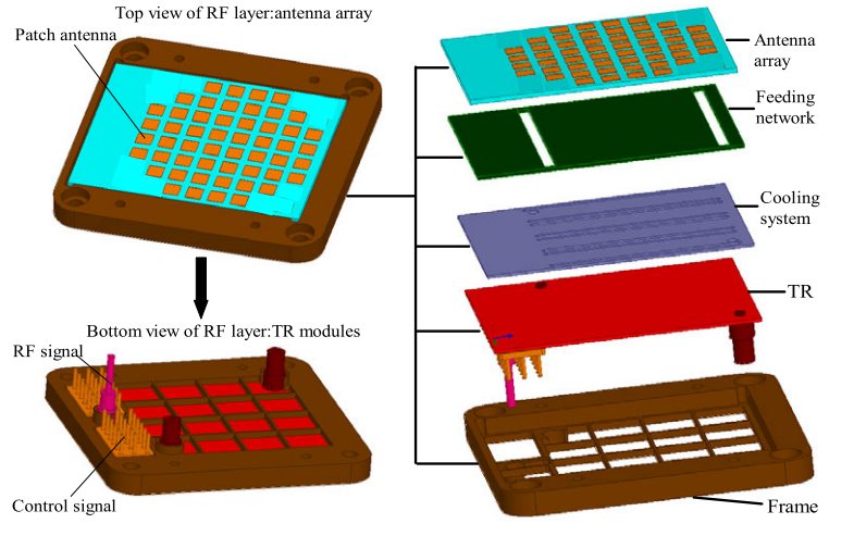
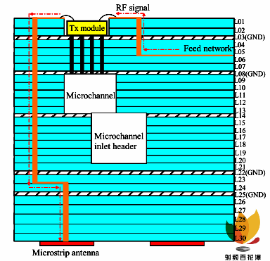
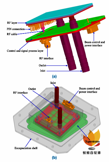
Figure 1 shows the schematic diagram of the antenna array system. The system consists of a package layer, a RF layer and a processing layer. The package layer includes the DC voltage source which supplies the power required by the phased array, and can simultaneity achieve impact and envi-ronmental resistances. The RF layer provides the receiving and transmitting function in the RF regime, which consists of a micro-strip antenna array, tile-style TR modules, a micro-channel cooling system and a strip-line feeding network. The processing layer comprises mainly the beam control circuit and the processing chip which generates the controlling sig-nal to realize beam scanning.
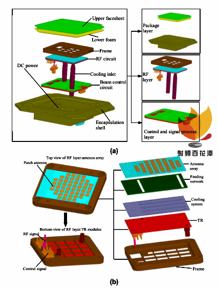
FIGURE 1. Schematic diagram of structurally integrated phased array.(a) Overall structural configuration. (b) Exploded view of the RF layerstructure.
B. DESIGN OF ACTIVE ANTENNA ARRAY WITH SUPERSTRATES
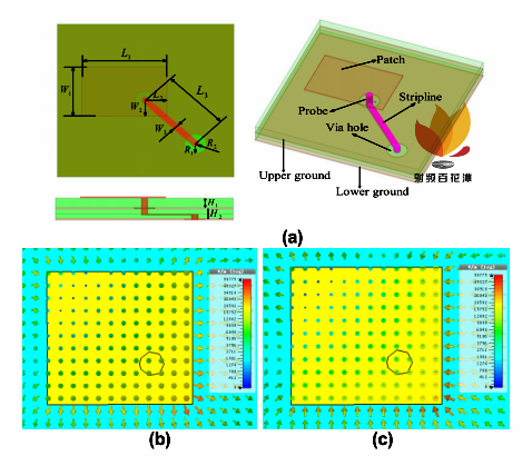
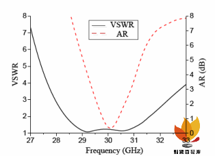
The simulated voltage standing wave ratio (VSWR) and axial ratio (AR) are plotted in Fig. 3. It is observed that the impedance bandwidth with VSWR < 2 is 10.8%(28.3-31.6 GHz) and the AR bandwidth with AR < 3dB isapproximately 5.0% (29.4-30.9GHz). The antenna element is left-hand circular polarization (LHCP) and has a peak simulated gain of 6.23 dBi at 30 GHz.
Based on the single antenna element above, a 52-element antenna array is constructed, as shown in Fig. 4. The 52 antenna elements are arranged into a rectangular array, which occupies a total area of 46 mm×44 mm. As shown in Fig. 4, sequential rotation feeding scheme is adopt in the 2 × 2 sub-array.
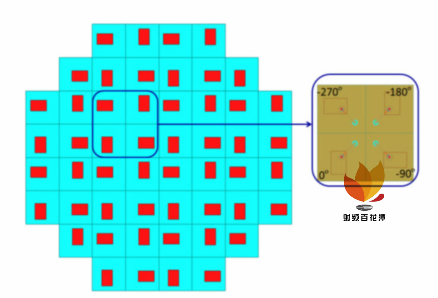
In order to improve the circularly polarized performance, the fourantenna element are rotated with respect to each other and excited with 90 ◦ phase difference increments, and the phase shifts are introduced by the phase shifters in the Tx modules. The distance between the elements is 5 mm, which is a half of the wavelength in free space at 30 GHz. Figure 5(a) presents the simulated radiation patterns of the antenna array at 30 GHz. It is observed that the antenna array has a peak gain of 21.6 dB and the side-lobe levels (SLL) are about -15 dB in the ±45 ◦ sweeping scope. The patterns in xoz and yoz planes are shown in Fig. 5(b) and Fig. 5(c), respectively. It is observed that the antenna array has a peak gain of 21.5 dBi and the cross-polarization levels are below -20 dBc. Besides, the side-lobe levels (SLL) in xoz-plane and yoz-plane are about -18.1 and -18.3 dBc, respectively.
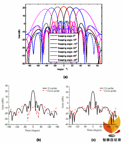
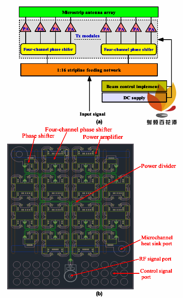
Figure 6(a) shows the block diagram of the active antenna array. The input RF signal is divided by a 1:16 stripline feeding network. The feeding network with a thickness of 4 LTCC layers contains fourstage Wilkinson dividers illustrated in Fig. 6(b). Simulated results show that the input VSWR of the feeding network is below 1.5 over the frequency range from 28 to 31.8 GHz, the phase imbalance of output ports is less than 1.6 degree, and the power imbalance is about 0.3 dB. Then, the output signals of the dividers are shifted in phase and amplified by power amplifiers in the Tx modules. The active Tx modules are composed of 16 sets of transmitter chips. As shown in Fig. 6 (b), each of the transmitter chipsets at the four corners of the board consist of a 6-bit digital phaseshifter and a power amplifier, and each of the other 12 chipsets consist of four-phase shifter and four power amplifiers. A 1:4 power divider and four 5-bit digital phase-shifters are incorporated in the multi-channel phase shifter. Finally, the output RF signals are fed to each element of the antenna array. Compared with conventional RF transmitter chip sets with a phase shifter and a power amplifier for each antenna element, the proposed RF front end has less integrated chips and occupies a smaller area.
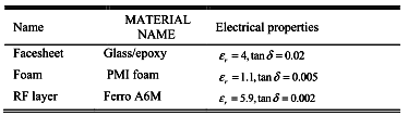
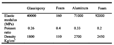
Subsequently, the next step is to determine the super-strates composed of the upper face-sheet and lower foam depicted in Fig. 7. The thickness of the super-strates locating above the antenna array not only contributes to the structural stiffness and strength, but also influences the electromagnetic performance. In order to meet the mechanical and electrical requirements simultaneously, the electromechanical co-design method is developed to design the super-strates.Tables 1 and 2 give the electrical and mechanical properties of the materials used in the antenna structure.
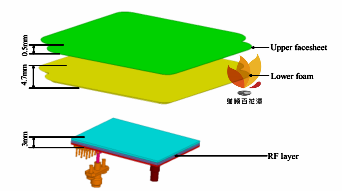
The coarse thicknesses of the facesheet and foam are optimized by the electromechanical co-design method in .The coarse thickness can provide an optimal structural stiffness and strength. However, it cannot guarantee an optimal design for the electromagnetic performance of the antenna array with the super-strates.In the last step, the coarse dimensions were applied to develop a full-wave electromagnetic model using the commercial simulation software HFSS from ANSYS. The thicknesses of the face-sheet and foam were further optimized and the final dimensions of the super-strates are determined as indicated in Fig. 7.
As mentioned above, high-power amplifiers are adopted in the Tx modules to enhance the signal power level. However, each amplifier is a heat source, which could influence the electrical performance of the active antenna array. In this work, a micro-channel heat sink is designed to cool the RF front end. Figure 8 shows the structural configuration of the micro-channel heat sink which consists of a micro-channel inlet header and a micro-channel outlet header, eight small micro-channels, an inlet and an outlet.
The micro-channel heat sink is fabricated based on the LTCC technology, and it is convenient to integrate the micro-channel heat sinks into the RF layer. However, because of a low heat transfer coefficient of the LTCC, it is slow to cool the RF layer. Therefore, under each high-power amplifier, a copper cylinder is utilized to connect the high-power ampli-fier (heat source) with the small micro-channel. Figure 8(c) shows the cross section of a micro-channel in the RF layer. The diameter and height of the copper cylinder are 1 and 1.2 mm, respectively. The coolant from the inlet flows into the micro-channel inlet header, and then is shunted into eight small micro-channels. The heat passes through the copper cylinder to the coolant, and then the coolant from the small micro-channels meets at the outlet header and flows away from the outlet. Utilizing the coolant movements, the heat is dissipated from the RF layer.

With the same coolant, the greater the flow rate of the coolant, the better the heat dissipation. Moreover, the more uniform the flow rate of the coolant in different micro-channels,the more uniform the temperature distribution in RF layer. The non-uniformity of the temperature distribution in the RF layer can lead to an inconsistent amplitude and phase variations of radiating element excitations which deteriorate the electrical performance of the active antenna array.In order to obtain a uniform temperature distribution,two schemes are designed, analyzed and compared in the following.
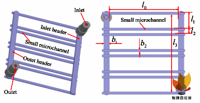
Figure 9 shows the geometry structure of micro-channel heat sinks. The cross section of the micro-channel heat sink is rectangle. The length, width and height of the inlet header and outlet header are 40 mm, 2.2 mm and 0.8 mm, respectively. The length, width and height of the small micro-channel are 36 mm, 1mm and 0.6 mm, respectively. The detailed dimensions of the optimized parameters in Fig. 10 are as follows (unit: mm): l 0 = 36, l 1 = 8, l 2 = 3, l 3 = 40,b 1 = 2.2, b 2 = 1. Numerical simulations are conducted to obtain the temperature fields of two schemes for the micro-channel heat sinks. Tables III and IV give the material properties and boundary conditions required by the simulation software ANSYS CFX. Figure 10 presents the temperature field distributions of structurally integrated active antenna. It can be observed from Fig. 10 that the temperature scope is from 48.04 ◦ C to 60.17 ◦ C.
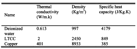
TABLE 4. Boundary conditions for numerical simulations.
TABLE 5. Statistical results of the temperature distribution.
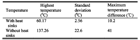
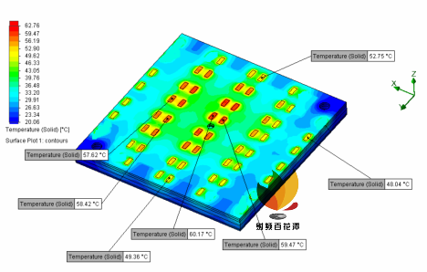
Table 5 gives the statistical results of the temperature dis-tributions on the surface of the RF layer. It also provides the standard deviation of the temperature and maximum temperature difference, which quantitatively evaluate the uniformity of the temperature distribution with and without heat sinks. The small deviation of the temperature and maximum temperature difference will cause smaller amplitude and phase variations of the radiating element excitations, which can provide a stable antenna electrical performance. From Tab. 5, it is obviously concluded that the scheme with heat sinks can provide a more uniform temperature distribution than that without the heat sinks. The impact from the heat sinks on the performance of the array system is discussed in Sec. V.
This section presents the fabrication of the structurally integrated phased array prototype. In the first step, according to the design above, the LTCC technology was exploited to fabricate the RF layer. In this work, the RF layer is made of 25 layers Ferro A6M tapes and 5 layers copper tapes (GND). Figure 11 presents a cross section of the 30 layers tapes layout. The micro-channel heat sinks are laminated with 12 layer tapes. The methods based on sacrificial volume materials (SVM) are applied to fabricate the micro-channels, and the SVM materials (i.e. carbon-black paste) are applied to fill in the micro-channels before the green tapes were sintered. The LTCC process begins with punching the via holes in the green ceramic tapes. Then, the via holes are metallized followed by the conductor patterning on each tape layer separately. Conductors are patterned using screen-printing techniques. After the tape sheets are aligned and laminated,the ceramic sheets are co-fired at the 850 ◦ ,and then the SVM evaporates in a pressurized environment of the high temperature, which shapes the resulting micro-channels. Finally, the transmitter chips are welded to the surface of the RF layer. The wire-bonding technique is applied to realize the interconnection between the Tx modules and the feeding network. Figures 12(a) and (b) show the front view and back view of the RF layer specimen, respectively, and the length, width and thickness of the specimen are 46 mm, 44 mm and 2.8 mm, respectively.
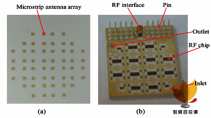
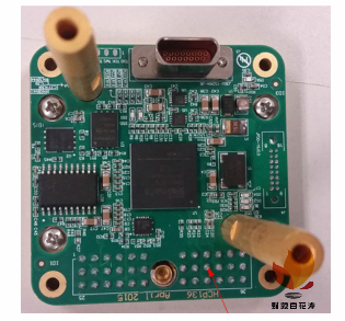
Then, the fabricated control and signal process layer is shown in Fig. 13. First, the beam control circuit is fabricated by using the PCB manufacturing technology. Then, the pin connections are applied to realize the interconnection between the beam control circuit and the DC power. The interconnections are conducted to form an initial assembly of the active antenna array without the package layer. The connections of different layers are shown in Fig. 14. Figure 14(a) shows the interconnection between the RF layer and the control and signal process layer, and two groups of pins (36 pins in all) are applied to connect the RF chips and the beam control circuit. Figure 14(b) shows the interface between the RF layer and external devices. The control and signal process layer is removed from the drawing, to allow a deeper insight into the structure. The inlet and the outlet which connect the RF layer and external devices, go through the control and signal process layer. The wire crosses the DC power, and connects the beam control circuit and an external computer terminal. Finally, the package layer is fabricated, and the antenna and the package layer are integrated to form the final antenna prototype by using the composite technology. In this step, the package layer consists of the encapsulate shell and the super-strates is made of aluminum to improve the structural stiffness and strength. The super-strate consists of the lower foam and the radome which is composited by the upper facesheet. After the package layer is fabricated, the active antenna array in the step 3 is put inside the encapsulate shell as shown in 14.
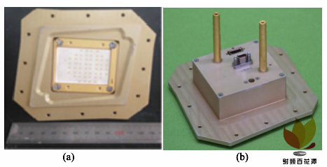
The encapsulate shell is made of aluminum to improve the structural stiffness and strength. The super-strate consists of the lower foam and the radome which is composited by the upper facesheet. After the package layer was fabricated, the active antenna array in the step3 was put inside the encapsulate shell as shown in Fig.15(a). Subsequently, the radome, the lower foam and the active antenna were bonded by using the composite technology. Each component is bonded on the top or bottom of another one in designed sequence. Figure 15 shows the fabricated antenna prototype.
In this section, experiments are carried out to validate the electromagnetic performance. To demonstrate the electro-magnetic performance, the radiation characteristics of the fabricated antenna prototype were measured in an anechoic chamber. Figure 16 shows the measured and simulated gain and AR against frequency of the antenna prototype. It is observed that the measured 3-dB gain band width ranges from about 28.5 GHz to 32 GHz with a peak gain of 21.0 dBi, while the 3-dB AR bandwidth is from around 28 GHz to 32.2 GHz. The measured and simulated results are overall in good agreement, and the discrepancy is due to the fabrication tolerance and measurement errors.
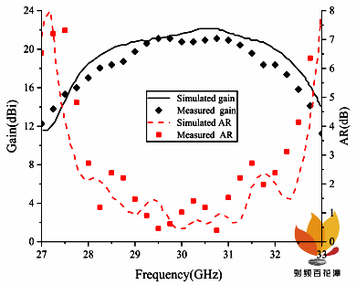
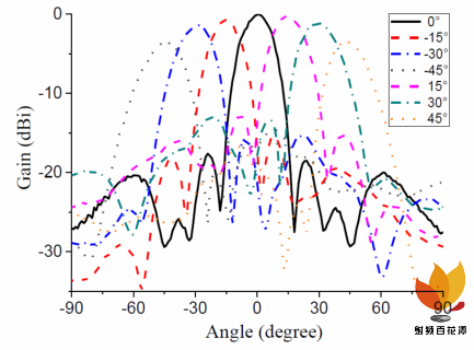
Figure 17 plots the scanning patterns in the azimuth plane at 30 GHz.The measured scanning range is from −45 ◦ to 45 ◦ ,and the measured beam direction exhibits slight difference from the expected scanning angle (−45 ◦ to +45 ◦ ). This difference may be due to the imperfections of the measurement system such as the phase error caused by the cables, adapters and alignment issues. The gain fluctuations within the scanning range are smaller than 3.5 dB, and the sidelobe levels are better than -12 dB. Moreover, it is found that the gain fluctuation is less than 1.5 dB when the scanning angle ranges from −30 ◦ to +30 ◦ . When the scanning angle is beyond±30 ◦ ,the gain drops by more than 3dB. This could be attributed to the roll-off of the antenna element patterns that get flattened due to the mutual coupling between the radiating elements.
The AR performance of array is also measured. As shown in Fig.18,the ARs are below 3 dB within the 3 dB beam width of the main beam, when the main beam is steered to 0, 15, 30 and 45 ◦ 。
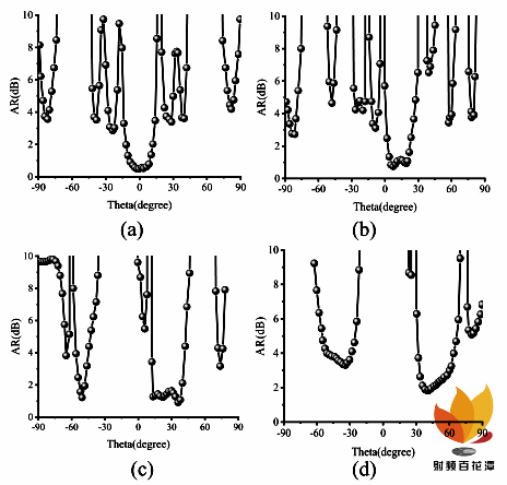
FIGURE 18. Measured axial ratio with beam scanned to different angles
at 30GHz, (a) θ = 0 ◦ , (b) θ = 15 ◦ , (c) θ = 30 ◦ , (d) θ = 45 ◦ (ϕ = 0 ◦ plane).
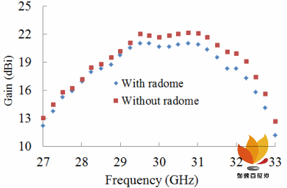
The mechanical structures and the thermal effects do affect the performance of the array.There are two mechanical structures that affect array performance. One is the radome and the other is the radiator. The other one is the heat sinks. The function of the radome is to protect the antenna front. However, after the radome is introduced, the matching between the array and free space is destroyed, so that the radiation efficiency of the array will be reduced, and eventually the radiation efficiency of the array will be reduced. Therefore,there is a trade-off between radome design and radiation efficiency. The material of the radome should have low dielectric constant to reduce the impact on the matching of the antenna to free space. At the same time, the radome should be low lossy to reduce dielectric loss.In our work,the material of the upper sheet of the radome is glass with ε r = 4, tanδ = 0.02,while the lower sheet of the radome is foam with ε r = 1.1,tanδ = 0.005. Figure 19 shows the change in gain with and without radome. It can be seen from Fig. 19 that with a radome, the array gain will drop, however, above 30 GHz, the gain decreases less than 2 dBi.
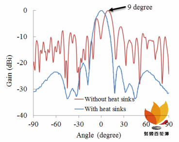
The heat sink structure does not directly affect the electrical performance of the antenna. The micro-channel heat sink is designed to cool the RF front end. Without the heat sink, as shown in Tab. 5, the highest temperature in the RF layer reaches 137◦ C. At such high temperature, solid-state devices at the RF layer cannot work properly. When the phased array works for a long time without heat dissipation structure, the amplitude and phase consistency of the RF channel deteriorate,and part of RF channels are even damaged.Therefore,the heat sink will indirectly affect the performance of the array. Figure 20 shows the radiation pattern of the array with and without a heat sink. It can be observed that, without heat sinks, the side lobe of the pattern is raised, and the main lobe pattern deviates under the condition of in-phase feeding. The array is no longer working properly. Insummary, the heat dis-sipation structure is particularly important for arrays. Owing to the heat sinks, the temperature in the RF layer is controlled within the operating temperature of the solid-state device.
This work presents the design, fabrication and testing of a Ka-band structurally integrated phased array. The electrome-chanical co-design methods are applied to design the package layer, the control and signal process layer and an RF layer. Thermal analysis of the RF layer is also carried out. The effects of mechanical structure and thermal effects on the performance of the antenna array are analyzed. The measurement results demonstrate the feasibility of the structurally integrated active antenna for airborne wireless communications. (参考文献略)

欢迎射频微波雷达通信工程师关注公众号

电子万花筒平台自营:Xilinx ALTERA ADI TI ST NXP 镁光 三星 海力士内存芯片 等百余品牌的电子元器件,可接受BOM清单,缺料,冷门,停产,以及国外对华禁运器件业务!
欢迎大家有需求随时发型号清单,我们将在第一时间给您呈上最好的报价,微信(QQ同号):1051197468 也希望您把我们的微信推荐给采购同事,感谢对平台的支持与信任!
与我们合作,您的器件采购成本将相比原有供应商降低10%以上!!不信?那您就来试试吧!!欢迎来撩!!