如需详细资料,请关注公众号并留言,或联系15321520153(同微信),邮箱cugboy311@126.com。

三河建华高科有限责任公司成立于2003年6月13日,隶属中国电子科技集团公司第四十五研究所。公司地处北京东燕郊经济技术开发区海油大街253号,占地100亩;公司现有总资产1.668亿元,资产负债率0.4%,银行信用等级AA+。公司现有各类技术人员60余人,高级技术职称15人。 三河建华高科有限责任公司以打造“中国半导体制造设备的引领者”为目标,致力于半导体元器件材料加工和芯片制造及检测专用设备的研究开发与生产制造,倾力建设华北地区高精密机械、光学、电器零部件制造中心。一、曝光设备
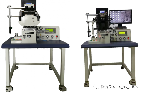
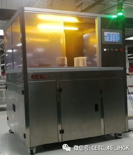
主要用于中小规模集成电路和半导体元器件制造工艺中的对准及曝光。本产品操作方便、稳定性高、重复性好,并具有较高的性能价格比,可广泛应用于科研和生产。
The machine is mainly used for alignment and exposure in process of small and middle scale IC. It is easy to operate, high stability, good repeatability, can be widely used in scientific research and production.主要技术指标 Main Specifications | |
| |
| |
| Separation Gap Between Substrate and Mask | |
| |
| |
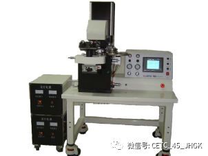
主要用于中小规模集成电路和半导体元器件制造工艺中的对准及曝光。本产品采用LED光源,操作方便、稳定性高、重复性好,并具有较高的性能价格比,可广泛应用于科研和生产。
The machine is mainly used for alignment and exposure in process of small and middle scale IC. It is use LED light source, easy to operate, high stability, good repeatability, can be widely used in scientific research and production.主要技术指标 Main Specifications | |
| |
| |
| Separation Gap Between Substrate and Mask | |
| |
| |
| 1.5μm(Positive PR Vacuum contact) |
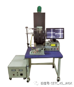
该设备主要用于半导体光电器件、功率器件、传感器、混合电路、微波器件及微电子机械系统(MEMS)等领域的双面对准和曝光。The machine is mainly designed by double aligning and exposure process of photoelectric device, power device, sensors, hybrid circuits,micro wave device and MEMS etc.主要技术指标 Main Specifications | |
| |
| |
| |
| Mask to Substrate Alignment Accuracy | ±3μm(Single-face two-mark detection) |
| 3μm(Positive PR)5μm(Negative PR) |
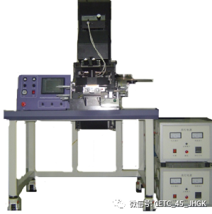
BG-406系列曝光机主要用于中小规模集成电路、二极管、三极管、GPP器件、LED、电力电子器件、MEMS和其它半导体器件制造工艺中的对准和曝光。该系列曝光机包括4″、6″单/双面曝光机,可实现单/双面对准、单面曝光。The series of BG-406 Mask Aligners could be used in aligning and exposure process of small or middle scale IC, Diode, dynatron, GPP, LED, Power Electronic devices, etc. The series of Mask Aligners include 4″,6″single/double sides aligning and single side exposure.主要技术指标 Main Specifications主要用于中小规模集成电路和半导体元器件制造工艺中的对准及曝光。本产品操作方便、稳定性高、重复性好,并具有较高的性能价格比,可广泛应用于科研和生产。The machine is mainly used for alignment and exposure in process of small and middle scale IC. It is easy to operate, high stability, good repeatability, can be widely used in scientific research and production.主要技术指标 Main Specifications | |
| |
| |
| Separation Gap Between Substrate and Mask | |
| |
| 1.5um(Positive PR, vacuum contact) |
该设备主要用于半导体光电器件、功率器件、传感器、混合电路、微波器件及微电子机械系统(MEMS)等领域的双面对准和曝光。The machine is mainly designed by double aligning and exposure process of photoelectric device, power device, sensors, hybrid circuits,micro wave device and MEMS etc.主要技术指标 Main Specifications | |
| |
| |
| |
| Mask to Substrate Alignment Accuracy | ±3μm(Single-face two-mark detection) |
| 6um(The thickness of positive PR and film is not more than 1μm) |
该设备为全自动曝光设备,主要用于中小规模集成电路和半导体元器件制造工艺中的对准及曝光。本产品自动完成基片的传输、对准与曝光工艺,操作方便、生产效率高、稳定性高。The machine is a full-automatic exposure, mainly used for alignment and exposure in process of small and middle scale IC. Automatically completes the transmission, alignment and exposure process of substrate, which is convenient for operation, high production efficiency and high stability.主要技术指标 Main Specifications | |
| |
| |
| |
| 260 wafer/h (first exposure, exposure time 3s) |
| | |
| | 2μm (Contact exposure, positive PR thick 1μm)
|
二、探针测试设备
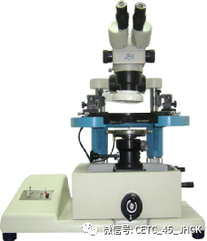
ST-103A型手动探针测试台
ST-103A Manual Probe
该设备是手动型探针台。它与测试仪连接后,主要用于各种半导体器件芯片的电参数测试,适用于科研分析用途、及小批量生产及抽测。
The equipment is a manual probe. After it is connected with the tester, it is mainly used for testing the electrical parameters of semiconductor chips. It is suitable for scientific research and analysis, small batch production and sampling test.

主要技术指标
□可测片径:3"、4"、5"、6"
□工作台行程:154mm×154mm
□工作台操作方式:手轮
□承片台Z向行程:2mm
□θ向调节范围:±45°
□显微镜:双目体视、放大倍数14×~90×
□照明:LED环形灯
□上、下片方式:手动方式
□外形尺寸:600mm×460mm×510mm
□重量:约50Kg
特殊配置
□ 可配高倍率显微镜(可选);
□ 可加装视频显示系统(可选)
□ 可配电磁屏蔽柜(可选)
□ 可配8”吸片盘、加热温控吸片盘(可选)
Main Specifications
□ Wafer Size:3"、4"、5"、6"
□ Working Stage Travel:154mm×154mm
□ Working Stage Operation: handwheel
□ Chuck Z-axis Travel: 2mm
□ θ Rotation Angle:±45°
□ Microscope: Magnification 14×~90×□ Lighting: LED ring lamp
□ Manual Load/Unload
□ Outline Dimension:600mm×460mm×510mm
□ Weight: 50Kg
Special Configure
High magnification microscope (optional);
Video display system (optional)
EMI shield (optional)
8 "chuck and heating temperature control (optional)
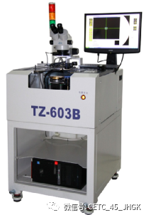
TZ-603B自动探针测试台
TZ-603B Automatic Probe
该设备是高速、高精度机型,具有高可靠性。主要适于半导体分立器件,光电器件以及集成电路芯片的测试。它与测试仪连接后,能自动完成对芯片的电参数测试及功能测试。
The equipment is a high-speed, high-precision model with high reliability. It is mainly suitable for testing discrete devices, photoelectric devices and IC. After it is connected with the tester, it can automatically test the electrical parameters and functions of the chip.

主要技术指标
□可测片径:4"、5"、6"
□步距范围:0.005mm~100mm
□工作台最大行程:180mm×240mm
□工作台速度:≥200mm/s
□定位精度:≤±0.01mm/160mm
□步进分辨率:0.001mm
□承片台Z向行程:10mm
□Z向定位精度:≤±0.003mm
□Z向分辨率:0.001mm
□θ向调节范围:±10°
□θ向分辨率:0.0013°
□观察装置:双目体视显微镜放大倍数14×~90×
□上、下片方式:手动或自动方式
□外形尺寸:700mm×800mm×1500mm
Main Specifications
□Wafer Size:4",5",6"
□Step Distance:0.005mm~100mm
□Max. Travel Range:180mm×240mm
□X/Y Axis Speed:≥200mm/s
□Positioning Accuracy:≤±0.01mm/160mm
□Resolution:0.001mm
□Chuck Z-axis Travel:10mm
□Z-axis Positioning Accuracy:≤±0.003mm
□Z-axis Resolution:0.001mm
□θ Rotation Angle:±10°
□θ Resolution:0.0013°
□Magnification:14×~90×□Manual Load/Unload
□Outline Dimension:700mm×800mm×1500mm
TZ-603C自动探针测试台
TZ-603C Automatic Probe
该设备是CCD自动对准的高性能自动机型,主要适用于GPP及其它晶圆的测试。它与测试仪连接后,能自动完成对芯片的电参数测试及功能测试。
The equipment is a high-performance automatic model of CCD alignment, which is mainly suitable for GPP and other wafer testing. After it is connected with the tester, it can automatically test the electrical parameters and functions of the chip.

主要技术指标
□可测片径:3"、4"、6"
□步距范围:0.005mm~100mm
□工作台最大行程:180mm×240mm
□工作台速度:≥200mm/s
□定位精度:≤±0.03mm/160mm
□步进分辨率:0.001mm
□承片台Z向行程:10mm
□Z向定位精度:≤±0.003mm
□Z向分辨率:0.001mm
□θ向调节范围:±10°
□θ向分辨率:0.0013°
□显微镜:单筒远心定倍显微镜;
□换挡变倍体视显微镜1×、3×(可选)
□CCD自动扫描时间:12s
□上、下片方式:手动方式
□外形尺寸:700mm×800mm×1500mm
Main Specifications
□Wafer Size:3"、4"、6"
□Step Distance:0.005mm~100mm
□Max. Travel Range:180mm×240mm
□X/Y Axis Speed:≥200mm/s
□Positioning Accuracy:≤±0.03mm/160mm
□Resolution:0.001mm
□Chuck Z-axis Travel:10mm
□Z-axis Positioning Accuracy: ≤±0.003mm
□Z-axis Resolution:0.001mm
□θRotation Angle:±10°
□θResolution:0.0013°
□Microscope: monocular fixed magnification
□Step Microscope 1×、3×(optional)
□Alignment Time:12s
□Manual Load/Unload
□Outline Dimension:700mm×800mm×1500mm
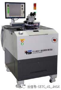
TZ-803A自动探针测试台
TZ-803A Automatic Probe
该设备主要用于半导体分立器件,光电器件以及集成电路晶圆上各个芯片的电参数分析、测试。该设备配接测试仪后,能自动完成芯片的电参数测试功能。
The equipment is mainly used for the analysis and test of the electrical parameters of discrete devices, photoelectric devices and IC. After it is connected with the tester, it can automatically test the electrical parameters and functions of the chip.

主要技术指标
□可测片径:5″、6″、8″
□工作台最大行程:240mm×300mm
□定位精度:≤±0.010mm/200mm
□工作台最大速度:200mm/s
□步进分辨:0.001mm
□承片台Z向行程:20mm
□Z向定位精度:≤±0.003mm
□Z向分辨率:0.001mm
□θ向调节范围:±6°
□θ自动对准精度:≤±0.01°
□步距范围:0.005mm~100mm
□观察装置:显微镜放大倍数14×~90×
□外形尺寸:750mm×1250mm×1600mm
Main Specifications
□Wafer Size:5"、6"、8"
□Max. Travel Range:240mm×300mm
□X/Y Positioning Accuracy:≤±0.010mm/200mm
□X/Y Axis Speed:200mm/s
□X/Y Resolution:0.001mm
□Chuck Z-axis Travel:20mm
□Z-axis Positioning Accuracy: ≤±0.003mm
□Z-axis Resolution:0.001mm
□θ Rotation Angle:±6°
□Alignment Accuracy: ≤±0.01°
□Step Distance:0.005mm~100mm
□Magnification:14×~90×□Outline Dimension:750mm×1250mm×1600mm
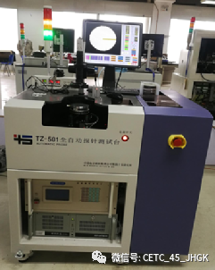
TZ-501全自动探针测试台
TZ-501 Automatic Probe
该设备为全自动设备,主要用于半导体分立器件GPP芯片的电参数分析、测试。该设备配接测试仪后,能自动完成芯片的电参数测试功能。
The equipment is fully automatic, which is mainly used for the analysis and test of the electrical parameters of the discrete device and GPP chip. After it is connected with the tester, it can automatically test the electrical parameters and functions of the chip.

主要技术指标
□可测片径:5″
□工作台最大行程:170mm×240mm
□定位精度:≤±0.030mm/150mm
□工作台速度:≥200mm/s
□步进分辨率:0.001mm
□承片台Z向行程:10mm
□Z向重复定位精度:≤±0.003mm
□Z向分辨率:0.001mm
□θ向自动调节范围:±10°
□θ向分辨率:0.0013°
□料盒移动行程:200mm
□机械手XY行程:100mm×200mm
□机械手θ向:0°~90°
□步距范围:0.005mm~100mm
□CCD光源调节方式:手动调节
□上、下片方式:机械手自动方式
□外形尺寸:1000mm×800mm×1500mm
Main Specifications
□Wafer Size:5"
□Max. Travel Range:170mm×240mm
□X/Y Positioning Accuracy:≤±0.030mm/150mm
□X/Y Axis Speed: ≥200mm/s
□X/Y Resolution:0.001mm
□Chuck Z-axis Travel:10mm
□Z-axis Positioning Accuracy:≤±0.003mm
□Z-axis Resolution:0.001mm
□θ Rotation Angle:±10°
□θResolution:0.0013°
□Cassette Range:200mm
□Manipulator XY Range: 100mm×200mm
□Manipulator θ Range: 0°~90°
□Step Distance: 0.005mm~100mm
□CCD light Adjustment : manual
□Load and unload: automatic mode
□Outline Dimension:1000mm×800mm×1500mm
TZ-502双工位全自动探针测试台
TZ-502 Double station automatic probe
该设备为双工位全自动设备,主要用于半导体分立器件GPP芯片的电参数分析、测试。该设备配接测试仪后,能自动完成芯片的电参数测试功能。
The equipment is double station fully automatic, which is mainly used for the analysis and test of the electrical parameters of the discrete device and GPP chip. After it is connected with the tester, it can automatically test the electrical parameters and functions of the chip.

主要技术指标
□可测片径:5″
□工作台最大行程:170mm×240mm
□定位精度:≤±0.030mm/150mm
□工作台速度:≥200mm/s
□步进分辨率:0.001mm
□承片台Z向行程:10mm
□Z向重复定位精度:≤±0.003mm
□Z向分辨率:0.001mm
□θ向自动调节范围:±10°
□θ向分辨率:0.0013°
□料盒移动行程:200mm
□机械手XY行程:100mm×200mm
□机械手θ向:0°~90°
□步距范围:0.005mm~100mm
□CCD光源调节方式:手动调节
□上、下片方式:机械手自动方式
□外形尺寸:1000mm×800mm×1500mm
Main Specifications
□Wafer Size:5"
□Max. Travel Range:170mm×240mm
□X/Y Positioning Accuracy:≤±0.030mm/150mm
□X/Y Axis Speed: ≥200mm/s
□X/Y Resolution:0.001mm
□Chuck Z-axis Travel:10mm
□Z-axis Positioning Accuracy:≤±0.003mm
□Z-axis Resolution:0.001mm
□θ Rotation Angle:±10°
□θResolution:0.0013°
□Cassette Range:200mm
□Manipulator XY Range: 100mm×200mm
□Manipulator θ Range: 0°~90°
□Step Distance: 0.005mm~100mm
□CCD light Adjustment : manual
□Load and unload: automatic mode
□Outline Dimension:1000mm×800mm×1500mm
三、匀胶显影设备
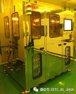
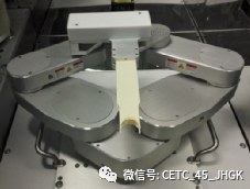
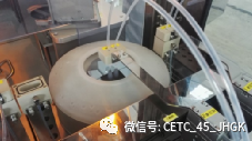
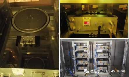
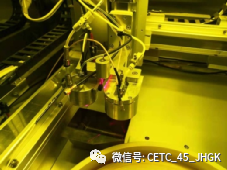
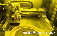
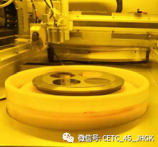
DYX-430SY Automatic Coater该设备主要用于LED、MEMS、IC等行业标准晶圆匀胶、预烘工艺。The equipment is mainly used for wafer coater and pre baker process in LED, MEMS, IC, etc.Adopt star layout, compact structure and high efficiency.Aluminum standard cassette, no deformation, easy to turn.选用进口多关节双臂机械手,不仅具有较高的刚度、灵活性,而且传输速度快,定位精度高。The imported multi joint double arm bobot not only has high rigidity and flexibility, but also has fast transmission speed and high positioning accuracy.匀胶腔采用进口PP材料制成,主轴电机采用进口定制的中空轴交流无刷伺服电机,保证旋转转速、加速度控制精度高,重复性、稳定性好。The cup is made of imported PP material. The spindle motor adopts the imported customized hollow AC brushless servo motor, ensure high accuracy, repeatability and stability of rotation speed and acceleration control.冷板/热板单元是对晶圆进行预烘及冷却处理,晶圆与盘体为非直接接触方式,温度稳定、精度高。The CP/HP unit is to pre bake and cool the wafer. The wafer and the plate are not in direct contact, stable temperature and high precision.Main Specifications of DYX-430SY| 主轴转速:0~6000rpm,最小调整量:1rpm温度均匀性:±1℃@50℃~120℃、±2℃@120.1℃~180℃外形尺寸:L1750mm×W1600mm×H1900mm | Spindle Speed: 0~6000rpm, min. adjustment: 1rpmSpeed Accuracy: ±1rpm(50~5000rpm)Spindle Acceleration: 100~20000rpm/secPR Supply: precision PR pumpPR Supply Accuracy: ±0.1mlTemperature Range: room temperature ~180℃Heating Method: mica heatingTemperature Uniformity: ±1℃@50℃~120℃,±2℃@120.1℃~180 ℃Cooling Mode: factory cooling waterWater Temperature Range: 18℃~30℃Outline Dimension: L1750mm×W1600mm ×H1900mm |
DYX-420SY Automatic Coater该设备为星型全自动匀胶设备,主要应用于4″或5″晶圆涂胶、预烘工艺。采用标准片盒收放片,工艺过程单片处理,自动运行,主要适用于分立器件、功率器件等领域。The equipment is a star type fully automatic coater. It is mainly used in 4 ″ or 5 ″ wafer coating and pre baker process. Adopt the standard cassette, single-chip processing, automatic operation. It is mainly suitable for discrete devices, power devices, etc.传输机构采用机械手进行晶圆的承载及传输,性能稳定,对晶圆背面污染小。The transfer unit adopts robot to carry and transmit the wafer, which has stable performance and little pollution to the back of the wafer.采用不锈钢匀胶腔体,中空轴伺服电机,具有密闭腔盖,保证匀胶过程中不产生胶丝。It adopts stainless steel cup, hollow axis servo motor and sealed cup cover to ensure that no glue wire is produced in the process of coater.Adopt hard anodizing hot plate, heat evenly, easy to wipe.Main Specifications of DYX-420SY| 主轴转速:0~5000rpm,最高:5000rpm温度均匀性:±2℃@50℃~100℃、±3℃@100.1℃~180℃外形尺寸:L1400mm×W1200mm×H1800mm | Number of Up / Down Cassette: 4 (two up and two down)Spindle Speed: 0~5000rpm, maximum: 5000rpmSpeed Accuracy: ±2rpm(50~5000rpm)PR Supply (Teflon Pump): 1~10mlPR Supply Accuracy: ±0.1mlTemperature Range: room temperature~180℃±1℃Temperature Uniformity: ±2℃@50℃~100℃, ±3℃@100.1℃~180℃Outline Dimension: L1400mm×W1200mm×H1800mm |
DYX-430Y Automatic Coater该设备为手动上下片,自动滴胶设备,可完成匀胶后烘焙工艺。最大适用5″标准晶圆,主要应用于分立器件、功率器件等行业。The equipment is a manual up and down wafer, automatic PR dropping equipment, which can complete the baking process after coater. It is applicable to 5 " wafer, mainly used in discrete devices, power devices and other industries.采用不锈钢匀胶腔体,中空轴伺服电机,具有密闭腔盖,保证匀胶过程中不产生胶丝。It adopts stainless steel cup, hollow axis servo motor and sealed cup cover to ensure that no glue wire is produced in the process of coater.Fast temperature rise, good baking effect, with hump structure, convenient for manual access.PR is supplied by precise PR pump with high precision and stable and reliable liquid supply.Main Specifications of DYX-430Y| 主轴转速:0~5000rpm,最高:5000rpm外形尺寸:L1500mm×W1000mm×H1800mm | Cup Material: stainless steelSpindle Speed: 0~5000rpm, maximum: 5000rpmSpeed Accuracy: ±2rpm(50~5000rpm)PR Supply (Teflon pump): 1~10mlPhotoresist supply accuracy: ± 0.1mlTemperature Range: 50~150℃Outline Dimension: L1500mm×W1000mm×H1800mm |
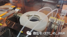
该产品适用于具有崎岖表面的异形基片表面光刻胶涂覆,主要应用于MEMS、陶瓷器件等领域。It is suitable for PR coating on the surface of special-shaped substrate with rugged surface, mainly used in MEMS, ceramic devices and other fields.采用超声或二流体喷头进行光刻胶雾化,光刻胶采用专用精密供液泵供给,精度高,供液稳定可靠。Ultrasonic or two fluid spray nozzle is used for PR spray. PR is supplied by special pump with high precision and stable liquid supply.XYZ轴工作台采用精密电缸驱动,无污染,扫描速度及加速度精度高、稳定性好。XYZ axis worktable is driven by precision electric cylinder, no pollution, high accuracy of scanning speed and acceleration, good stability.主轴电机采用交流无刷伺服电机,保证旋转转速、加速度控制精度高,稳定性好;加热机构采用接触式烘焙,加热控制精度高,温度均匀性好。The main spindle motor adopts AC servo motor to ensure high accuracy and stability of rotation speed and acceleration control; the HP adopts contact baking, with high accuracy of heating control and good temperature uniformity.Main Specifications of DYX-810P| 外形尺寸:L1500mm×W960mm×H1600mm | Spindle Speed: 0~200rpm, rated: 100rpmSpeed Accuracy: ±1rpm(0~100rpm)PR Supply Accuracy: ±0.1mlMaximum Speed of X: 200mm/sMaximum speed of Y: 200mm/sTemperature Range: 50~150℃Temperature Uniformity: ±3℃Outline Dimension: L1500mm×W960mm×H1600mm |
DYX-640S Automatic Coater & Developer该设备主要用于LED、MEMS、IC等行业标准晶圆匀胶、、显影、预烘工艺。The equipment is mainly used for wafer coater developer and pre baker process in LED, MEMS, IC, etc.Adopt star layout, compact structure and high efficiency.Aluminum standard cassette, no deformation, easy to turn.选用进口多关节双臂机械手,不仅具有较高的刚度、灵活性,而且传输速度快,定位精度高。The imported multi joint double arm bobot not only has high rigidity and flexibility, but also has fast transmission speed and high positioning accuracy.匀胶腔采用进口PP材料制成,主轴电机采用进口定制的中空轴交流无刷伺服电机,保证旋转转速、加速度控制精度高,重复性、稳定性好。The cup is made of imported PP material. The spindle motor adopts the imported customized hollow AC brushless servo motor, ensure high accuracy, repeatability and stability of rotation speed and acceleration control.显影腔特殊结构设计可实现废液收集、气流控制等功能,使显影工艺条件达到最佳。The developer cup can realize the functions of waste liquid collection, air flow control, etc., so as to optimize the developing process conditions.冷板/热板单元是对晶圆进行预烘及冷却处理,晶圆与盘体为非直接接触方式,温度稳定、精度高。The CP/HP unit is to pre bake and cool the wafer. The wafer and the plate are not in direct contact, stable temperature and high precision.Main Specifications of DYX-640S| 主轴转速:0~6000rpm,最小调整量:1rpm温度均匀性:±1℃@50℃~120℃、±2℃@120.1℃~180℃外形尺寸:L1950mm×W1700mm×H1900mm | Spindle Speed: 0~6000rpm, min. adjustment: 1rpmSpeed Accuracy: ±1rpm(50~5000rpm)Spindle Acceleration: 100~20000rpm/secPR Supply: precision PR pumpPR Supply Accuracy: ±0.1mlDeveloper Quantity: 2 setsNozzle Type: column or H typeSupply Mode: stainless steel pressure tankTemperature Range: room temperature ~180℃Heating Method: mica heatingTemperature Uniformity: ±1℃@50℃~120℃,±2℃@120.1℃~180 ℃Cooling Mode: factory cooling waterWater Temperature Range: 18℃~30℃Outline Dimension: L1750mm×W1600mm ×H1900mm
|
四、内圆切片设备
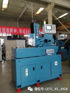
QP Series of Inner Circle Slicer该系列产品主要用于半导体材料、玻璃、陶瓷、钽酸锂、闪烁晶体、碲锌镉等脆硬材料的切割。This series of products are mainly used for cutting brittle and hard materials such as semiconductor materials, glass, ceramics, lithium tantalite, scintillation crystal, CdZnTe, etc.Main Specifications of QP-301D | | Diameter of Cutting Ingot | |
| | | |
| | Max. Length of Cutting Ingot | |
| | | |
| | | |
| | Adjustment of Horizontal Crystal Direction | |
| | Adjustment of Vertical Crystal Direction | |
| φ422mm规格加深型刀盘配置方案,使刀厚设定范围最大可达58mm(QP-301T)。 | φ 422mm deepened blade plate makes the maximum setting range of cutter thickness reach 58mm (QP-301T). |
| φ457mm规格刀盘配置方案,使切割晶棒最大直径可达φ105mm(QP-401)。 | φ 457mm blade plate can make the maximum diameter to φ 105mm (QP-401). |
Main Specifications of QP-613B | | Diameter of Cutting Ingot | |
| | | |
| | Max. Length of Cutting Ingot | |
| | | |
| | | |
| | Adjustment of Horizontal Crystal Direction | |
| | Adjustment of Vertical Crystal Direction |
|


