微影技术的研发已进展至极短波长的超紫外光(EUV),来自美国马里兰大学(University of Maryland)的研究团队则提出一种多光子光阻剂(multi-photon photoresists),能让可见光微影达到纳米等级的分辨率;通常微影分辨率是与曝光时间成反比。
“大多数达到高分辨率微影的方法,都是与采用更短波长的光源有关;”马里兰大学教授John Fourkas表示:“我们的目标是以可见光产出纳米级的微影效果。”该团队新开发的多光子技术简称 RAPID (Resolution Augmentation through Photo-Induced Deactivation,透过光致去活化达到的分辨率强化方法),以一道激光在光阻剂中启动曝光,然后加入第二道激光来完成整个程序,仅在两个聚焦光束重迭的纳米等级范围内进行完全曝光。
Fourkas指出:“只要我们用一道激光并透过显微镜物镜来进行聚焦,我们就能把吸收作用(absorption)局限在激光聚焦体积的微小区域中。”研究人员已经就芯片上3D材料的选择性聚合作用(selective polymerization),将该技术优化;利用一种“多光子吸收聚合作用(Multi-photon Absorption Polymerization,MAP)”,研究团队在芯片上制作出了微小的电感。
RAPID则是后续的工作,利用光阻剂的多光子吸收作用,来达成聚焦可见光微影的纳米等级分辨率,可望延缓甚至可能免除采用超紫外光源的需要。

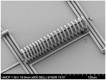
图中是采用多光子吸收聚合作用(MAP)、接着又以选择性金属化(selective metallization)所制作的微电感(microinductor)
这种技术适用于标准的大气压力条件,不像深紫外光需要在真空中操作;该光阻剂中特有的光启动程序(photo-initiator)是由一道激光所活化,然后再被第二道激光去活化,证实了研究人员称之为PROVE (proportional velocity)的现象,也就是更高的曝光度可产出更小的特征尺寸。
接下来研究人员计划以晶圆片尺寸规格来测试其技术,突破到目前为止都是以逐点(point-by-point)方式进行的实验;而该研究团队也估计,RAPID技术要迈入商业化阶段还需要约十年的时间。
翻译:Judith Cheng
点击进入参考原文:Multi-photon photoresists said to beat UV
《电子工程专辑》网站版权所有,谢绝转载
{pagination}
Multi-photon photoresists said to beat UV
R. Colin Johnson
As photolithography research moves toward extremely short wavelengths of ultra-violet light, one group at the University of Maryland is proposing multi-photon photoresists that allow visible light to achieve nanoscale resolution that is inversely dependent on exposure time.
"Most approaches to getting higher resolution with photolithography involve using light of ever shorter wavelengths," said professor John Fourkas. "Our goal is to use visible light to produce nanoscale features."
The new multi-photon technique, called Resolution Augmentation through Photo-Induced Deactivation (RAPID), uses one laser to initiate exposure in the photoresist and a second to complete it, allowing full exposure of only the nanoscale overlapping areas of the two focused beams.
"If we take a laser beam and focus it through a microscope objective," said Fourkas. "We can confine absorption to this very tiny region right at the focal volume of the laser."
The researchers have already perfected the technique for use in the selective polymerization of 3-D materials on-chip. Using what is called Multi-photon Absorption Polymerization (MAP), the team has fabricated tiny inductors on chips. RAPID is a follow-on effort to use multi-photon absorption with photoresists to achieve nanoscale resolution with focused visible light, delaying or possible eliminating the need to move to extreme ultra-violet light sources (EUV).
Microinductor created using multiphoton absorption polymerization (MAP) followed by selective metallization.
The technique works at normal atmospheric pressure, unlike EUV with requires processing in a vacuum. Instead, a special photo-initiator in the resist is activated by one laser, then deactivated by a second, realizing a phenomenon the researchers call proportional velocity (PROVE), which yields smaller features for higher exposures.
Next the researchers plan to test their technique of the wafer scale, in contrast to the point-by-point demonstrations they have given so far. The team estimates that RAPID will be ready for commercialization in about 10 years.