加拿大麦基尔大学(McGill Universtiy)的研究人员近来宣布一项技术突破,号称可大幅缩小有机半导体组件与硅芯片之间的性能差距。
与硅材料相较,有机半导体可采用较简易的低温工艺生产,所产出的器件不但成本比较低,并具备高度可调谐特性(tunable properties);但遗憾的是,有机材料的载子迁移率(carrier mobility)较差,使得其性能比传统的无机半导体组件差了一大截,幅度超过千倍。
而麦基尔大学的研究人员最近示范了一种能缩小有机半导体与无机材料之间性能差距的方法,是通过由下而上的自动组装(bottom-up self-assembly)技术,复制有机半导体的高度秩序化(highly ordered)纳米结构。

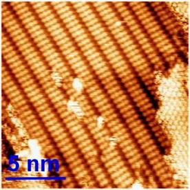
复制无机铜晶体排列秩序、以5纳米分辨率所制作的高分子聚合物
麦基尔大学教授Dmitrii Perepichkal表示:“我们的研究成果是取一种完美有序的无机材料晶体──在这里是单晶铜──然后将其秩序转化到一个有机层中;”他是与法国国家科学研究院(Institut national de la recherche scientifique)教授Federico Rosei一同进行上述研究。
“具体来说,我们成功展示了一种最重要的有机导电高分子聚合物──PEDOT (polyethylenedioxythiophene)──的完美秩序化数组。”Perepichkal表示。
研究人员通过复制已经具备完美晶体结构的铜薄膜,利用简易的低温沉积技术让单体(monomer,聚合物的成分)自动在无机材料上组装成聚合物。“当这些小小的单分子触及晶体的表面,它们就会以该晶体本身的排列模式聚合成最后的聚合物数组。”Perepichkal指出。
利用该结晶化PEDOT单层膜(monolayers)所制作的有机晶体管,在尺寸上可望比目前的半导体组件小十倍、但性能则可媲美诸如硅等无机材料。
这项研究目前还在早期阶段,但研究人员表示该技术最终可适用各种有机半导体组件的生产,应用范围包括大尺寸计算机显示器,以及高效益、廉价的塑料太阳能电池。而研究人员的下一步是将目前以1D方式(单层膜)呈现的成果,进展到传统芯片制造所使用的2D架构。
下一页:参考原文(Low-cost organic semiconductors said to rival silicon, by R. Colin Johnson )
《电子工程专辑》网站版权所有,谢绝转载
{pagination}
Low-cost organic semiconductors said to rival silicon
by R. Colin Johnson
University researchers have reported a breakthrough that could help organic semiconductors bridge the considerable performance gap with silicon chips.
Organic semiconductors offer easier low-temperature processing than silicon, resulting in lower cost semiconductors with highly tunable properties. Unfortunately, the poor carrier mobility of organic materials makes their performance characteristics lag behind traditional inorganic semiconductors by a thousand times or more.
The researchers at McGill Universtiy (Montreal) demonstrated a method of endowing organic semiconductors with the performance characteristics of inorganic materials by copying their highly ordered nanoscale structure with bottom-up self-assembly techniques.
"What we show in this work is that we can take a crystalline that is perfectly ordered inorganic material—here single crystal copper—and translate its order into that of an organic layer," said McGill professor Dmitrii Perepichkal, who performed the work with professor Federico Rosei at the Institut national de la recherche scientifique. "Specifically, we demonstrate perfectly ordered arrays of one of the most important organic conducting polymer, PEDOT [polyethylenedioxythiophene]."
The researchers attained five nanometer resolution for lines of PEDOT by copying the already perfect crystalline structure of thin-film copper, using a simple low-temperature deposition technique whereby "monomers" self-assembled into polymers atop the inorganic material.
"When these small monomer molecules—the constituents of a polymer—reach the surface of a crystal, they polymerize in such a way that the direction of the resulting polymer lines is defined by the crystal itself," said Perepichkal.
The crystalline monolayers of PEDOT hold the potential of enabling organic transistors to be ten time smaller than today's semiconductors, but with performance that rivals inorganic materials like silicon.
Although their work is still in the early stages, the researchers claim their technique could eventually be adapted to a wide variety of organic semiconductors including wide-area computer displays and highly efficient but inexpensive plastic solar cells.
So far the researchers have only demonstrated the effect in one dimensional, but are currently working to show it can be duplicated in traditional two-dimensional sheets, resulting in organic monolayers from which traditional electronic circuits can be fabricated.